C-11
REGISTERS
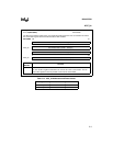
CCR0
CCR0
no direct access
†
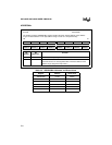
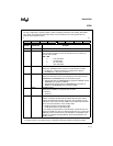
The chip configuration 0 (CCR0) register enables or disables powerdown and standby (80C196NU
only) modes and selects the write-control mode. It also contains the bus-control parameters for
fetching chip configuration byte 1.
7 0
1 1 WS1 WS0 DEMUX BHE# BW16 PD
Bit
Number
Bit
Mnemonic
Function
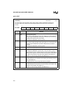
7:6 1 To guarantee device operation, write ones to these bits.
5:4 WS1:0 Wait States
These two bits control the number of wait states that are used for an
external fetch of CCB1.
WS0 WS1
0 0 zero wait states
0 1 one wait state
1 0 two wait states
1 1 three wait states
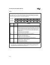
3 DEMUX Select Demultiplexed Bus
Selects the demultiplexed bus mode for an external fetch of CCB1:
0 = multiplexed — address and data are multiplexed on AD15:0.
1 = demultiplexed — data only on AD15:0.
2 BHE# Write-control Mode
Selects the write-control mode, which determines the functions of the
BHE#/WRH# and WR#/WRL# pins for external bus cycles:
0 = write strobe mode: the BHE#/WRH# pin operates as WRH#, and the
WR#/WRL# pin operates as WRL#.
1 = standard write-control mode: the BHE#/WRH# pin operates as
BHE#, and the WR#/WRL# pin operates as WR#.
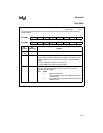
1 BW16 Buswidth Control
Selects the bus width for an external fetch of CCB1:
0 = 8-bit bus
1 = 16-bit bus
0 PD Powerdown Enable
Enables or disables the IDLPD #2 and IDLPD #3 instructions. When
enabled, the IDLPD #2 instruction causes the microcontroller to enter
powerdown mode and for the 80C196NU only, the IDLPD #3 instruction
causes the microcontroller to enter standby mode.
0 = disable powerdown and standby modes
1 = enable powerdown and standby modes
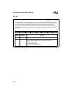
If your design uses powerdown or standby mode, set this bit when you
program the CCBs. If it does not, clearing this bit when you program the
CCBs will prevent accidental entry into powerdown and standby mode
†
.
(Chapter 12, “Special Operating Modes,” discusses powerdown and
standby modes.)
†
The CCRs are loaded with the contents of the chip configuration bytes (CCBs) after a device reset.
The CCBs reside in nonvolatile memory at addresses FF2018H (CCB0) and FF201AH (CCB1).


