13-11
INTERFACING WITH EXTERNAL MEMORY
13.3.3 Chip-select Unit Initial Conditions
A chip reset produces the following initial conditions for the chip-select unit:
• ADDRMSKx = XFFFH.
• ADDRCOM0 = 0F20H. This asserts CS0# for the 256-byte address range F2000–F20FFH.
• ADDRCOM1–ADDRCOM5 = X000H.
• For the fetch of chip configuration byte 0 (CCB0), BUSCON0 is initialized for an 8-bit bus
width, multiplexed mode, and three wait states (DEMUX = 0, BW16 = 0, WS0 = 1, WS1 =
1).
• Before the fetch of chip configuration byte 1 (CCB1), the values of DEMUX, BW16, WS0,
and WS1 in BUSCON0 are loaded from CCB0. The external bus is configured according to
the new values.
The first lines of your program should perform two tasks:
1. Set the stack pointer.
2. Initialize all of the chip-select registers (ADDRCOMx, ADDRMSKx, and BUSCONx, by
using the procedure in “Initializing the Chip-select Registers.”
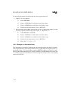
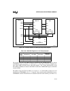
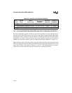
13.3.4 Initializing the Chip-select Registers
When initializing the chip-select parameters (or modifying them at any time), it is important to
avoid a condition in which two chip-selects outputs have overlapping address ranges and different
bus-parameter values (wait states, bus width, and multiplexing). Accessing a location in such an
overlapping address range can cause unpredictable results.
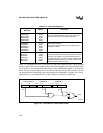
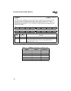
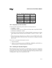
Table 13-7. BUSCON
x
Addresses and Reset Values
Register Address Reset Value
BUSCON0 1F44H 03H
BUSCON1 1F4CH 00H
BUSCON2 1F54H 00H
BUSCON3 1F5CH 00H
BUSCON4 1F64H 00H
BUSCON5 1F6CH 00H


