13-13
INTERFACING WITH EXTERNAL MEMORY
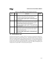
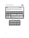
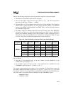
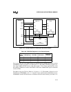
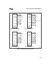
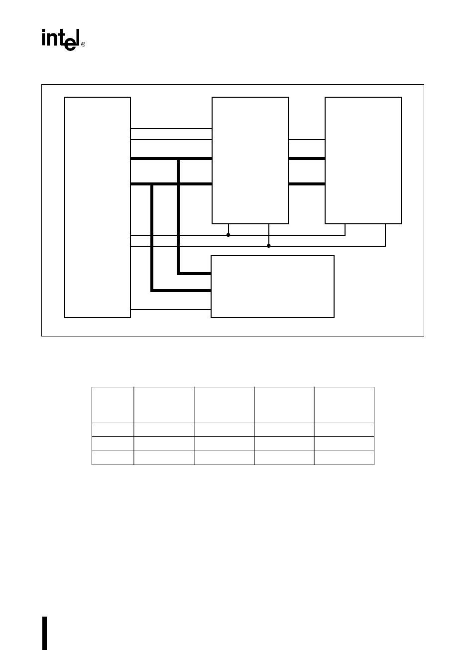
Figure 13-5. Example System for Setting Up Chip-select Outputs
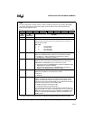
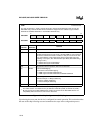
The location and size of an address range are specified by the ADDRCOMx register and the
ADDRMSKx register (see Figure 13-2 and Figure 13-3). The 8-Kbyte SRAM is assigned to ad-
dress range 7E000–7FFFFH and uses chip-select output 2. The 12 most-significant bits of the
base address (7E000H) are written to the BASE19:8 bits in the ADDRCOM2 register, which then
contains 07E0H.
The address range for CS2# is 8 Kbytes or 2
13
bytes (n = 13). The number of bits to be set in
MASK19:8 of ADDRMSK2 is 20 – n = 7. After the 7 most-significant bits of MASK19:8 are set,
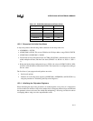
ADDRMSK2 contains 0FE0H. Results for CS0# and CS1# are found similarly (see Table 13-9).
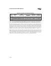
Table 13-8. BUSCON
x
Registers for the Example System
Chip-
select
Output
Multiplexing Bus Width Wait States
Contents of
BUSCON
x
0 Demultiplexed 16 bits 0 C0H
1 Demultiplexed 8 bits 3 83H
2 Demultiplexed 8 bits 0 80H
CS0#
CS2#
A19:0
AD15:0
RD#
WR#
CS1#
8XC196
CE#
D7:0
A2:0
0 WS
80000–FFFFFH
82510
UART
Flash
256K×16
SRAM
8K×8
CE#
A17:0
D15:0
0 WS
7E000–7FFFFH
A12:0
D7:0
CE#
WE#OE# WE#OE#
AD7:0
A2:0
A18:1
AD15:0
Txd
Rxd
A12:0
AD7:0
A2433-03
3 WS
01E00–01EFFH


