13-5
INTERFACING WITH EXTERNAL MEMORY
13.3 THE CHIP-SELECT UNIT
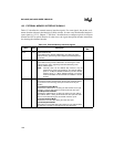
The chip-select unit provides six outputs, CS5:0#, for selecting an external device during an ex-
ternal bus cycle. During an external memory access, a chip-select output CSx# is asserted if the
address falls within the address range assigned to that chip-select. The bus width, the number of
wait states, and multiplexed or demultiplexed address/data lines are programmed independently
for each of the six chip-selects. If the external address is outside the range of the six chip-selects,
the chip-select 5 bus control register determines the wait states, bus width, and multiplexing, and
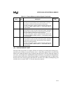
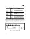
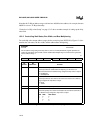
no chip-select is asserted. Table 13-3 lists the chip-select registers.
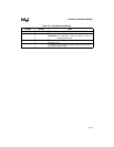
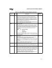
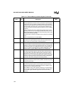
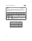
WR# O Write
†
This active-low output indicates that an external write is occurring.
This signal is asserted only during external memory writes.
†
The chip configuration register 0 (CCR0) determines whether this
pin functions as WR# or WRL#. CCR0.2 = 1 selects WR#; CCR0.2 =
0 selects WRL#.
WRL#
WRH# O Write High
†
During 16-bit bus cycles, this active-low output signal is asserted for
high-byte writes and word writes to external memory. During 8-bit
bus cycles, WRH# is asserted for all write operations.
†
The chip configuration register 0 (CCR0) determines whether this
pin functions as BHE# or WRH#. CCR0.2 = 1 selects BHE#; CCR0.2
= 0 selects WRH#.
P5.5/BHE#
WRL# O Write Low
†
During 16-bit bus cycles, this active-low output signal is asserted for
low-byte writes and word writes. During 8-bit bus cycles, WRL# is
asserted for all write operations.
†
The chip configuration register 0 (CCR0) determines whether this
pin functions as WR# or WRL#. CCR0.2 = 1 selects WR#; CCR0.2 =
0 selects WRL#.
WR#
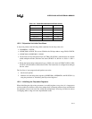
Table 13-2. External Memory Interface Signals (Continued)
Name Type Description
Multiplexed
With


