13-7
INTERFACING WITH EXTERNAL MEMORY
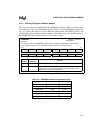
13.3.1 Defining Chip-select Address Ranges
This section describes the ADDRCOMx and ADDRMSKx registers and how to set them up for
a desired address range. The ADDRCOMx register (Figure 13-2) and ADDRMSKx register (Fig-
ure 13-3) control the assertion of each chip-select output CSx#. The BASE19:8 bits in the
ADDRCOMx register determine the base address of the address range. The MASK19:8 bits in
the ADDRMSKx register determine the size of the address range.
ADDRCOM
x
x
= 0–5
Address:
Reset State:
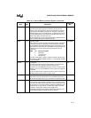
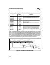
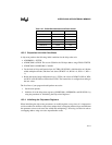
Table 13-4
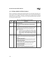
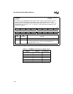
The address compare (ADDRCOM
x
) register specifies the base (lowest) address of the address
range. The base address of a 2
n
-byte address range must be on a 2
n
-byte boundary.
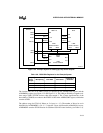
15 8
— — — — BASE19 BASE18 BASE17 BASE16
7 0
BASE15 BASE14 BASE13 BASE12 BASE11 BASE10 BASE9 BASE8
Bit
Number
Bit
Mnemonic
Function
15:12 — Reserved; for compatibility with future devices, write zeros to these bits.
11:0 BASE19:8 Base Address Bits
These bits are the 12 most-significant bits of the base address of the
address range assigned to chip-select
x
.
Figure 13-2. Address Compare (ADDRCOM
x
) Register
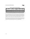
Table 13-4. ADDRCOM
x
Addresses and Reset Values
Register Address Reset Value
ADDRCOM0 1F40H 0F20H
ADDRCOM1 1F48H X000H
ADDRCOM2 1F50H X000H
ADDRCOM3 1F58H X000H
ADDRCOM4 1F60H X000H
ADDRCOM5 1F68H X000H


