8XC196NP, 80C196NU USER’S MANUAL
C-10
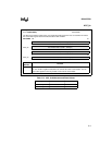
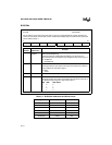
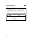
BUSCONx
BUSCON
x
x
= 0–5
Address:
Reset State:
Table C-7
For the address range assigned to chip-select
x
, the bus control (BUSCON
x
) register specifies the
number of wait states, the bus width, and the address/data multiplexing for all external bus cycles that
access address range
x
.
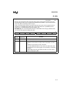
7 0
DEMUX BW16 — — — — WS1 WS0
Bit
Number
Bit
Mnemonic
Function
7 DEMUX Address/Data Multiplexing
This bit specifies the address/data multiplexing on AD15:0 for all
external accesses to the address range assigned to chip-select output
x
.
0 = multiplexed
1 = demultiplexed
6 BW16 Bus Width
This bit specifies the bus width for all external accesses to the address
range assigned to chip-select output
x
.
0 = 8 bits
1 = 16 bits
5:2 — Reserved; for compatibility with future devices, write zeros to these bits.
1:0 WS1:0 Wait States
These bits specify the number of wait states for all external accesses to
the address range assigned to chip-select output
x
.
WS1 WS0 Wait States
00 0
01 1
10 2
11 3
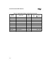
Table C-7. BUSCON
x
Addresses and Reset Values
Register Address Reset Value
BUSCON0 1F44H 03H
BUSCON1 1F4CH 00H
BUSCON2 1F54H 00H
BUSCON3 1F5CH 00H
BUSCON4 1F64H 00H
BUSCON5 1F6CH 00H


