8XC196NP, 80C196NU USER’S MANUAL
B-12
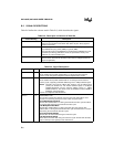
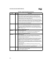
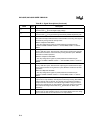
V
CC
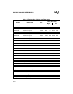
PWR Digital Supply Voltage
Connect each V
CC
pin to the digital supply voltage.
V
SS
GND Digital Circuit Ground
Connect each V
SS
pin to ground through the lowest possible impedance path.
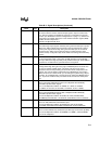
WR# O Write
†
This active-low output indicates that an external write is occurring. This signal is
asserted only during external memory writes.
WR# is multiplexed with WRL#.
†
The chip configuration register 0 (CCR0) determines whether this pin
functions as WR# or WRL#. CCR0.2 = 1 selects WR#; CCR0.2 = 0 selects
WRL#.
WRH# O Write High
†
During 16-bit bus cycles, this active-low output signal is asserted for high-byte
writes and word writes to external memory. During 8-bit bus cycles, WRH# is
asserted for all write operations.
WRH# is multiplexed with BHE#.
†
The chip configuration register 0 (CCR0) determines whether this pin
functions as BHE# or WRH#. CCR0.2 = 1 selects BHE#; CCR0.2 = 0 selects
WRH#.
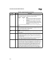
WRL# O Write Low
†
During 16-bit bus cycles, this active-low output signal is asserted for low-byte
writes and word writes. During 8-bit bus cycles, WRL# is asserted for all write
operations.
WRL# is multiplexed with WR#.
†
The chip configuration register 0 (CCR0) determines whether this pin
functions as WR# or WRL#. CCR0.2 = 1 selects WR#; CCR0.2 = 0 selects
WRL#.
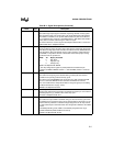
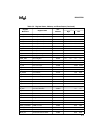
XTAL1 I Input Crystal/Resonator or External Clock Input
Input to the on-chip oscillator, internal phase-locked loop circuitry (80C196NU),
and the internal clock generators. The internal clock generators provide the
peripheral clocks, CPU clock, and CLKOUT signal. When using an external
clock source instead of the on-chip oscillator, connect the clock input to XTAL1.
The external clock signal must meet the V
IH
specification for XTAL1 (see
datasheet).
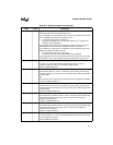
XTAL2 O Inverted Output for the Crystal/Resonator
Output of the on-chip oscillator inverter. Leave XTAL2 floating when the design
uses a external clock source instead of the on-chip oscillator.
Table B-3. Signal Descriptions (Continued)
Name Type Description


