9-10
8XC196NP, 80C196NU USER’S MANUAL
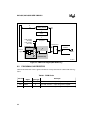
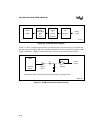
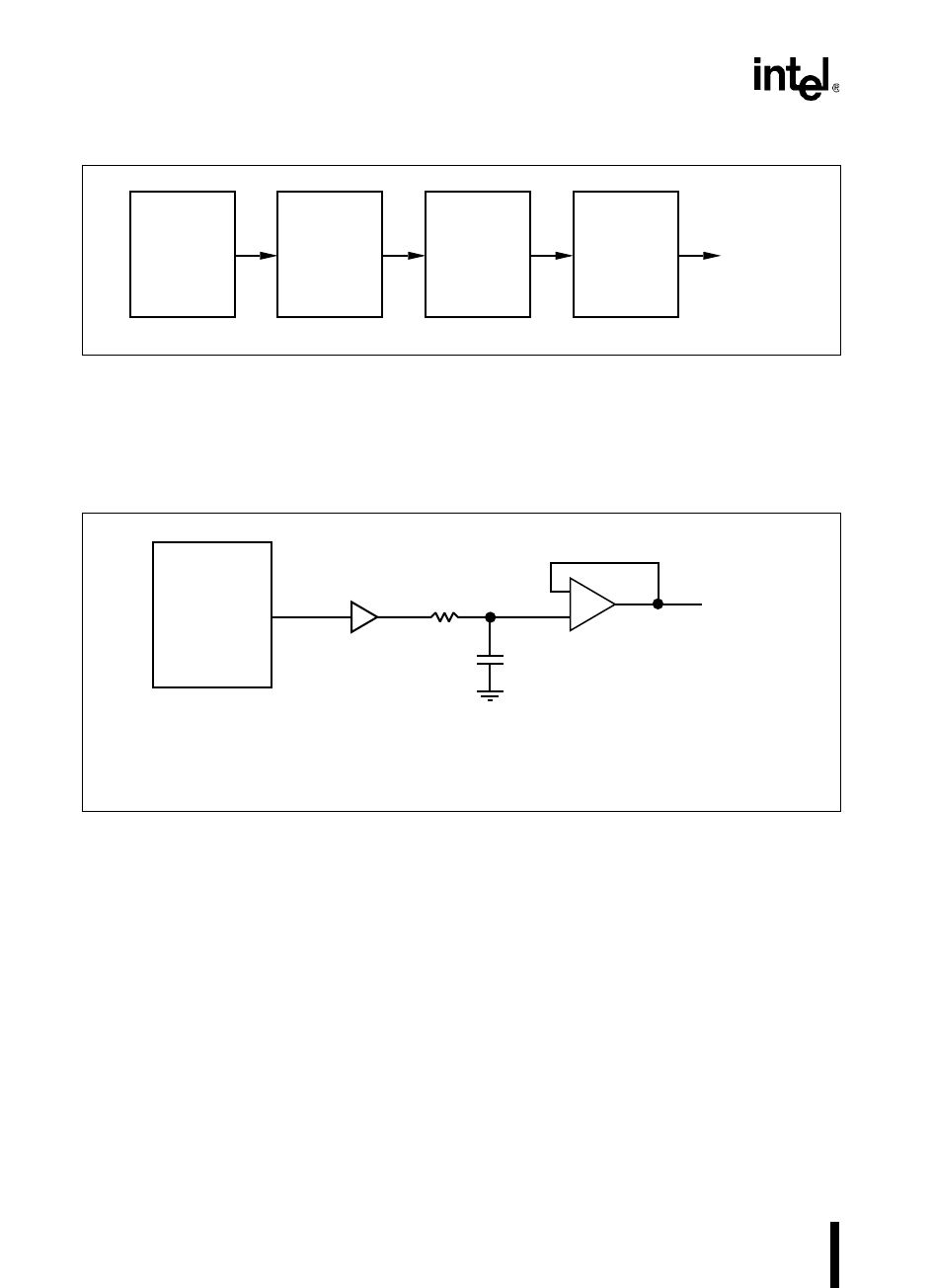
Figure 9-6. D/A Buffer Block Diagram
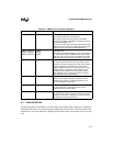
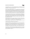
Figure 9-7 shows a sample circuit used for low output currents (less than 100 µA). Consider tem-
perature and power-supply drift when selecting components for the external D/A circuitry. With
proper components, a highly accurate 8-bit D/A converter can be made using the PWM.
Figure 9-7. PWM to Analog Conversion Circuitry
Buffer
to Make
Output Swing
Rail
to
Rail
8XC196
Device
PWM
Filter
(Passive
or
Active)
(Optional)
Power
Amp
(Optional)
Analog
Output
A2391-01
74ACxxx
Buffer
PWM
8XC196
Device
Analog
Output
Op Amp
R
C
-
+
A2390-02
Consider both ripple and response time requirements when selecting R and C.


