7-10
8XC196NP, 80C196NU USER’S MANUAL
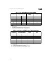
P2.7/CLKOUT Following reset, P2.7 carries the strongly driven CLKOUT signal. It
is not held high. When P2.7 is configured as CLKOUT, it is always a
complementary output.
P2.7 A value written to P2_REG.7 is held in a buffer until P2_MODE.7 is
cleared, at which time the value is loaded into P2_REG.7. A value
read from P2_REG.7 is the value currently in the register, not the
value in the buffer. Therefore, any change to P2_REG.7 can be read
only after P2_MODE.7 is cleared.
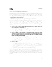
Port 3 After reset, your software must configure the device to match the
external system. This is accomplished by writing appropriate config-
uration data into P3_MODE. Writing to P3_MODE not only
configures the pins but also turns off the transistor that weakly holds
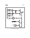
the pins high (Q4 in Figure 7-1 on page 7-5). For this reason, even if
port 3 is to be used as it is configured at reset, you should still write
data into P3_MODE.
P3.0/CS0# P3.0/CS0# is weakly pulled high during reset. After reset, it defaults
to the CS0# function. This chip-select signal detects address ranges
that contain the CCBs and FF2080H (program start-up address). See
Chapter 13, “Interfacing with External Memory,” for a detailed
description of chip-select signal functions after reset.
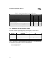
P3.6/EXTINT2 Writing to P3_MODE.6 sets the EXTINT2 interrupt pending bit
(INT_PEND1.5). After configuring the port pins, clear the interrupt
pending registers before globally enabling interrupts. See “Design
Considerations for External Interrupt Inputs” on page 7-11.
P3.7/EXTINT3 Writing to P3_MODE.7 sets the EXTINT3 interrupt pending bit
(INT_PEND1.6). After configuring the port pins, clear the interrupt
pending registers before globally enabling interrupts. See “Design
Considerations for External Interrupt Inputs” on page 7-11.
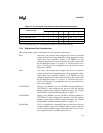
Port 4 After reset, your software must configure the device to match the
external system. This is accomplished by writing appropriate config-
uration data into P4_MODE. Writing to P4_MODE not only
configures the pins but also turns off the transistor that weakly holds
the pins high (Q4 in Figure 7-1 on page 7-5). For this reason, even if
port 4 is to be used as it is configured at reset, you should still write
data into P4_MODE.


