8XC196NP, 80C196NU USER’S MANUAL
13-16
Upon leaving the reset state, the device is configured for normal operation. This section describes
the state of the chip following reset and summarizes the steps in the configuration process.
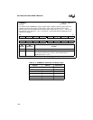
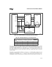
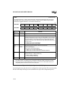
CCR1
no direct access
†
The chip configuration 1 (CCR1) register selects the 16-bit or 24-bit addressing mode and (for the
8XC196NP only) controls whether the internal ROM is mapped into two address ranges, FF2000–
FF2FFFH and 002000–002FFFH, or into FF2000–FF2FFFH only.
7 0
8XC196NP
1 101 1 REMAP MODE64 —
7 0
80C196NU
1 1DM1 1—MODE64 —
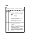
Bit
Number
Bit
Mnemonic
Function
7:6 1 To guarantee device operation, write ones to these bits.
5
††
DM Deferred Mode
Enables the deferred bus-cycle mode. If the 80C196NU is using a demulti-
plexed bus and deferred mode is enabled, a delay of 2t occurs in the first
bus cycle following a chip-select output change and the first write cycle
following a read cycle. (See “Deferred Bus-cycle Mode (80C196NU Only)”
on page 13-40.)
0 = deferred bus-cycle mode disabled
1 = deferred bus-cycle mode enabled
4:3 1 To guarantee device operation, write ones to these bits.
2
††
REMAP Internal ROM Mapping
Controls the internal ROM mapping.
0 = ROM maps to FF2000–FF2FFFH only
1 = ROM maps to FF2000–FF2FFFH and 002000–002FFFH
1 MODE64 Addressing Mode
Selects 64-Kbyte or 1-Mbyte addressing.
0 = selects 1-Mbyte addressing
1 = selects 64-Kbyte addressing
0 — Reserved; for compatibility with future devices, write zero to this bit.
†
The CCRs are loaded with the contents of the chip configuration bytes (CCBs) after a device reset.
The CCBs reside in nonvolatile memory at addresses FF2018H (CCB0) and FF201AH (CCB1).
††
Bit 5 is reserved on the 8XC196NP device and bit 2 is reserved on the 80C196NU device. For
compatibility with future devices, write zeros to these bits.
Figure 13-7. Chip Configuration 1 (CCR1) Register


