11-5
MINIMUM HARDWARE CONSIDERATIONS
Multilayer printed circuit boards with separate V
CC
and ground planes also help to minimize
noise. For more information on noise protection, refer to AP-125, Designing Microcontroller Sys-
tems for Noisy Environments and AP-711, EMI Design Techniques for Microcontrollers in Auto-
motive Applications.
11.4 THE ON-CHIP OSCILLATOR CIRCUITRY
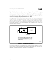
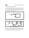
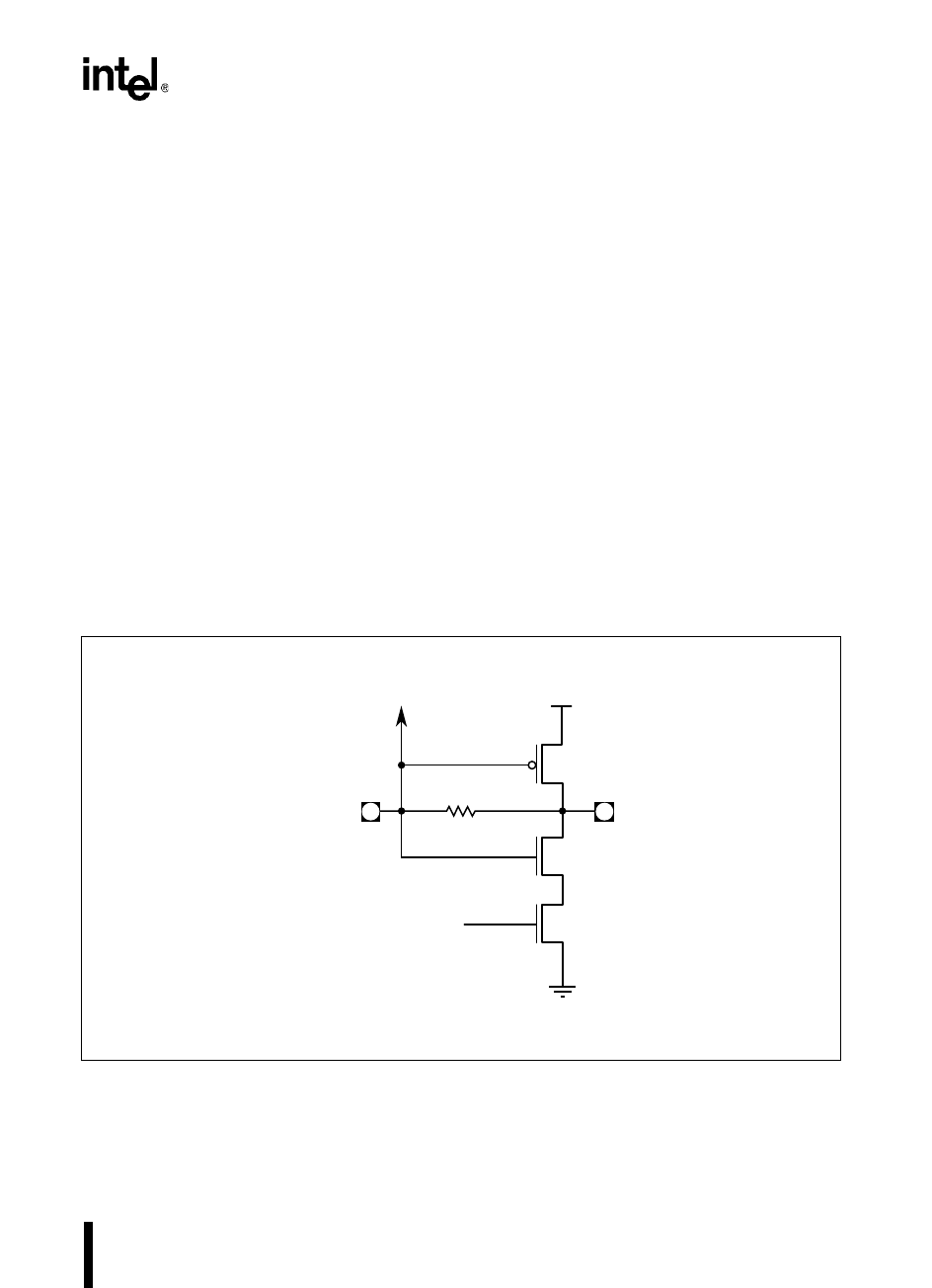
The on-chip oscillator circuit (Figure 11-3) consists of a crystal-controlled, positive reactance os-
cillator. In this application, the crystal operates in a parallel resonance mode. The feedback resis-
tor, Rf, consists of paralleled n-channel and p-channel FETs controlled by the internal powerdown
signal. In powerdown mode, Rf acts as an open and the output drivers are disabled, which disables
the oscillator. Both the XTAL1 and XTAL2 pins have built-in electrostatic discharge (ESD) pro-
tection.
NOTE
For the 80C196NU, although the maximum external clock input frequency is
50 MHz, the maximum oscillator input frequency is limited to 25 MHz.
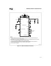
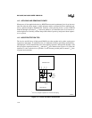
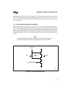
Figure 11-3. On-chip Oscillator Circuit
Rf
XTAL2
(Output)
V
CC
XTAL1
(Input)
Oscillator Enable#
(from powerdown circuitry)
To internal
circuitry
A0076-03
V
SS


