13-35
INTERFACING WITH EXTERNAL MEMORY
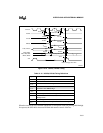
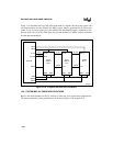
To write single bytes on a 16-bit bus requires separate low-byte and high-byte write signals
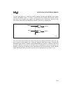
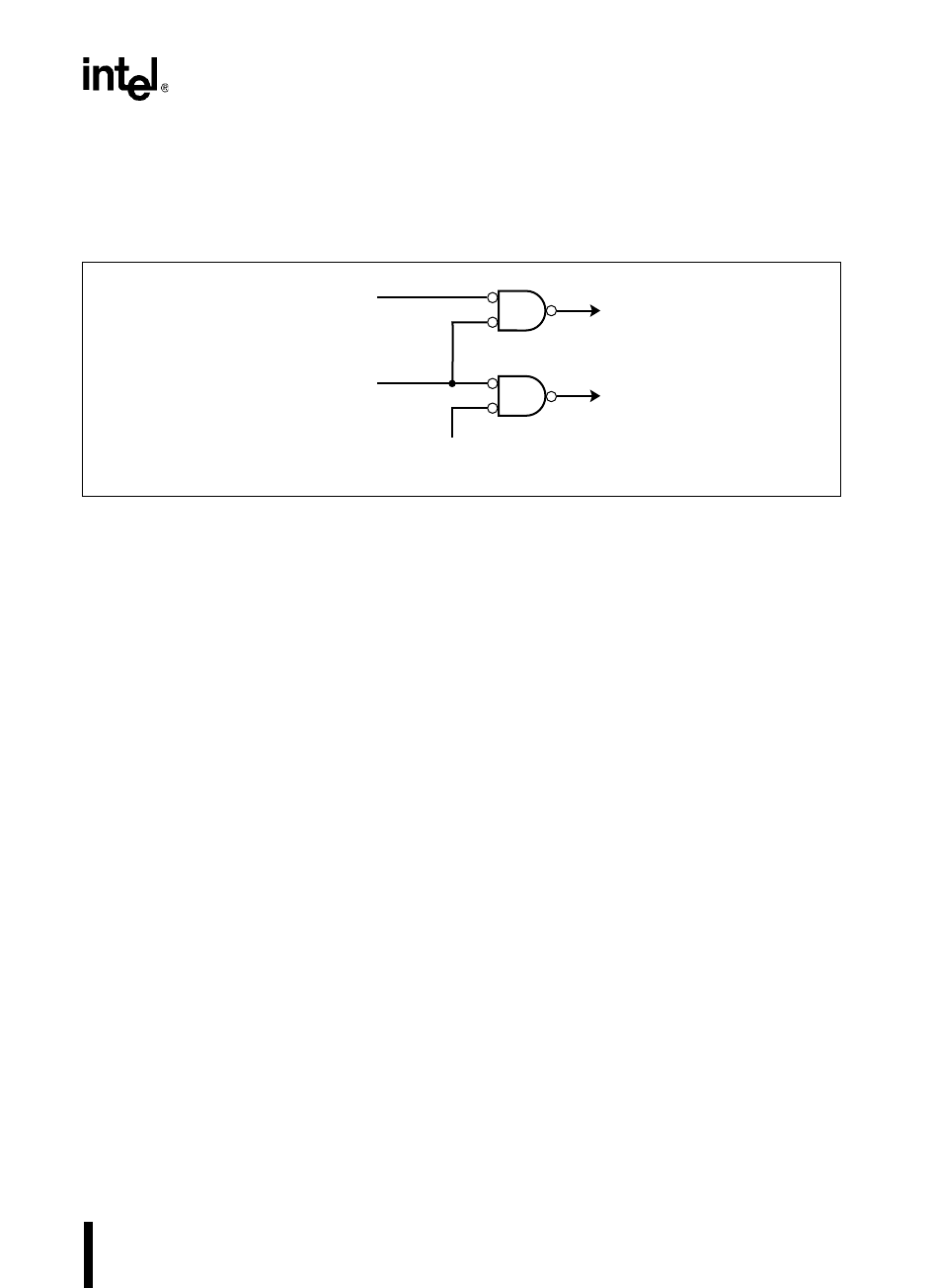
(WRL# and WRH#). Figure 13-18 shows a sample circuit that combines WR#, BHE#, and ad-
dress bit 0 (A0) to produce these signals. This additional logic is unnecessary, however. In the
write strobe mode, WRL# and WRH# are available at the device’s external pins.
Figure 13-18. Decoding WRL# and WRH#
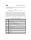
The write strobe mode eliminates the need to externally decode high-byte and low-byte write sig-
nals to external 16-bit memory on a 16-bit bus. When the write strobe mode is selected, the
WR#/WRL# pin operates as WRL#, and the BHE#/WRH# pin operates as WRH#. In the 16-bit
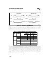
bus mode, WRL# is asserted for all low-byte writes (even addresses) and all word writes, and
WRH# is asserted for all high-byte writes (odd addresses) and all word writes. In the 8-bit bus
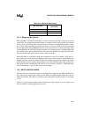
mode, WRH# and WRL# are asserted for both even and odd addresses (see Table 13-14).
BHE#
WR#
A0
WRH#
WRL#
A0104-01


