8XC196NP, 80C196NU USER’S MANUAL
6-30
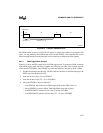
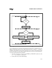
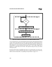
Figure 6-16 is a flow diagram of the EPA and PTS operations for this example. Operation begins
when the timer is enabled (at time = 0 in Figure 6-14 on page 6-27) by the write to T1CONTROL.
The first timer match occurs at time = T1. The EPA toggles the output pin to zero and generates
an interrupt to initiate the first PTS cycle.
PWM Toggle Cycle 1. Because TBIT is initialized to one, the PTS adds the off-time value
(T2 – T1) to EPA0_TIME and toggles TBIT to zero.
The second timer match occurs at time = T2 (the end of one complete PWM pulse). The EPA tog-
gles the output to one and generates an interrupt to initiate the second PTS cycle.
PWM Toggle Cycle 2. Because TBIT is zero, the PTS adds the on-time value (T1) to
EPA0_TIME and toggles the TBIT to one.
The next timer match occurs at time = T2 + T1. The EPA toggles the output to zero and initiates
the third PTS cycle. The PTS actions are the same as in cycle 1, and generation of the PWM output
continues with PTS cycle 1 and cycle 2 alternating.
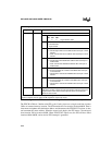
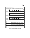
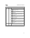
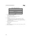
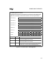
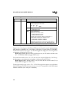
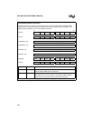
Register Location Function
PTSCON PTSCB + 1 PTS Control Bits
M2:0 PTS Mode
These bits specify the PTS mode:
M2 M1 M0
010PWM
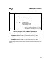
TMOD Toggle Mode Select
1 = PWM toggle mode
TBIT Toggle Bit Initial Value
Defines the initial value of TBIT.
0 = selects initial value as zero
1 = selects initial value as one
The TBIT value determines whether PTSCONST1 or
PTSCONST2 is added to the PTSPTR1 value:
0 = PTSCONST1 is added to PTSPTR1
1 = PTSCONST2 is added to PTSPTR1
Reading this bit returns the current value of TBIT, which is
toggled by hardware at the end of each PWM toggle cycle.
PTS PWM Toggle Mode Control Block (Continued)
Figure 6-15. PTS Control Block — PWM Toggle Mode (Continued)


