7-3
I/O PORTS
7.2.1 Bidirectional Port Operation
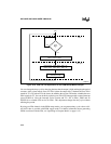
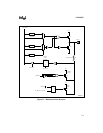
Figure 7-1 shows the logic for driving the output transistors, Q1 and Q2. On ports 1, 2, and 3, Q1
can source at least –3 mA at V
CC
– 0.7 volts. On port 4, which has a high-current sink capability
for the PWMs, Q1 can source at least –3 mA at 0.45 volts. Q2 can sink at least 10 mA at 0.45
volts. (Consult the datasheet for specifications.)
In I/O mode (selected by clearing Px_MODE.y), Px_REG and Px_DIR are input to the multiplex-
ers. These signals combine to drive the gates of Q1 and Q2 so that the output is high, low, or high
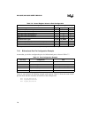
impedance. Table 7-4 is a logic table for I/O operation of these ports.
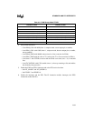
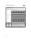
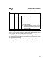
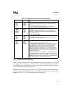
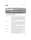
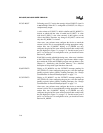
Table 7-3. Bidirectional Port Control and Status Registers
Mnemonic Address Description
P1_DIR
P2_DIR
P3_DIR
P4_DIR
1FD2H
1FCBH
1FDAH
1FDBH
Port
x
Direction
Each bit of P
x
_DIR controls the direction of the corresponding pin.
0 = complementary output (output only)
1 = input or open-drain output (input, output, or bidirectional)
Open-drain outputs require external pull-ups.
P1_MODE
P2_MODE
P3_MODE
P4_MODE
1FD0H
1FC9H
1FD8H
1FD9H
Port
x
Mode
Each bit of P
x
_MODE controls whether the corresponding pin
functions as a standard I/O port pin or as a special-function signal.
0 = standard I/O port pin
1 = special-function signal
P1_PIN
P2_PIN
P3_PIN
P4_PIN
1FD6H
1FCFH
1FDEH
1FDFH
Port
x
Input
Each bit of P
x
_PIN reflects the current state of the corresponding
pin, regardless of the pin configuration.
P1_REG
P2_REG
P3_REG
P4_REG
1FD4H
1FCDH
1FDCH
1FDDH
Port
x
Data Output
For an input, set the corresponding P
x
_REG bit.
For an output, write the data to be driven out by each pin to the
corresponding bit of P
x
_REG. When a pin is configured as standard
I/O (P
x
_MODE.
y
= 0), the result of a CPU write to P
x
_REG is
immediately visible on the pin. When a pin is configured as a
special-function signal (P
x
_MODE.
y
= 1), the associated on-chip
peripheral or off-chip component controls the pin. The CPU can still
write to P
x
_REG, but the pin is unaffected until it is switched back to
its standard I/O function.
This feature allows software to configure a pin as standard I/O (clear
P
x
_MODE.
y
), initialize or overwrite the pin value, then configure the
pin as a special-function signal (set P
x
_MODE.
y
). In this way, initial-
ization, fault recovery, exception handling, etc., can be done without
changing the operation of the associated peripheral.


