7-9
I/O PORTS
7.2.4 Bidirectional Port Considerations
This section outlines special considerations for using the pins of these ports.
Port 1 After reset, your software must configure the device to match the
external system. This is accomplished by writing appropriate config-
uration data into P1_MODE. Writing to P1_MODE not only
configures the pins but also turns off the transistor that weakly holds
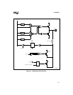
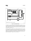
the pins high (Q4 in Figure 7-1 on page 7-5). For this reason, even if
port 1 is to be used as it is configured at reset, you should still write
data into P1_MODE.
Port 2 After reset, your software must configure the device to match the
external system. This is accomplished by writing appropriate config-
uration data into P2_MODE. Writing to P2_MODE not only
configures the pins but also turns off the transistor that weakly holds
the pins high (Q4 in Figure 7-1 on page 7-5). For this reason, even if
port 2 is to be used as it is configured at reset, you should still write
data into P2_MODE.
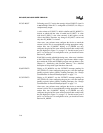
P2.2/EXTINT0 Writing to P2_MODE.2 sets the EXTINT0 interrupt pending bit
(INT_PEND.3). After configuring the port pins, clear the interrupt
pending registers before globally enabling interrupts. See “Design
Considerations for External Interrupt Inputs” on page 7-11.
P2.4/EXTINT1 Writing to P2_MODE.4 sets the EXTINT1 interrupt pending bit
(INT_PEND.4). After configuring the port pins, clear the interrupt
pending registers before globally enabling interrupts. See “Design
Considerations for External Interrupt Inputs” on page 7-11.
P2.5/HOLD# If P2.5 is configured as a standard I/O port pin, the device does not
recognize signals on this pin as HOLD#. Instead, the bus controller
receives an internal HOLD signal. This enables the device to access
the external bus while it is performing I/O at P2.5.
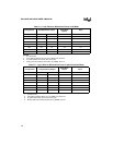
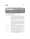
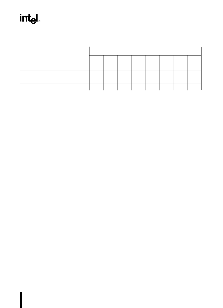
Table 7-8. Port Pin States After Reset and After Example Code Execution
Action or Code
Resulting Pin States
†
P
x
.7 P
x
.6 P
x
.5 P
x
.4 P
x
.3 P
x
.2 P
x
.1 P
x
.0
Reset wk1 wk1 wk1 wk1 wk1 wk1 wk1 wk1
LDB P
x
_DIR, #00011111B 1 1 1 wk1 wk1 wk1 wk1 wk1
LDB P
x
_MODE, #00000000B 1 1 1 HZ1 HZ1 HZ1 HZ1 HZ1
LDB P
x
_REG, #10010011B 1 0 0 HZ1 0 0 HZ1 HZ1
†
wk1 = weakly pulled high, HZ1 = high impedance (actually a “1” with an external pull-up).


