11-1
CHAPTER 11
MINIMUM HARDWARE CONSIDERATIONS
The 8XC196NP and 80C196NU have several basic requirements for operation within a system.
This chapter describes options for providing the basic requirements and discusses other hardware
considerations.
11.1 MINIMUM CONNECTIONS
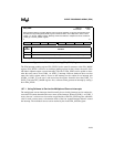
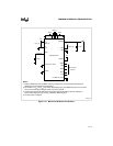
Table 11-1 lists the signals that are required for the device to function and Figure 11-1 shows the
connections for a minimum configuration.
Table 11-1. Minimum Required Signals
Signal
Name
Type Description
RESET# I/O Reset
A level-sensitive reset input to and open-drain system reset output from the micro-
controller. Either a falling edge on RESET# or an internal reset turns on a pull-down
transistor connected to the RESET# pin for 16 state times. In the powerdown,
standby, and idle modes, asserting RESET# causes the chip to reset and return to
normal operating mode. After a device reset, the first instruction fetch is from
FF2080H (or F2080H in external memory). For the 80C196NP and 80C196NU, the
program and special-purpose memory locations (FF2000–FF2FFFH) reside in
external memory. For the 83C196NP, these locations can reside either in external
memory or in internal ROM.
RPD I Return from Powerdown
Timing pin for the return-from-powerdown circuit.
If your application uses powerdown mode, connect a capacitor
†
between RPD and
V
SS
if either of the following conditions is true.
• the internal oscillator is the clock source
• the phase-locked loop (PLL) circuitry (80C196NU only) is enabled (see
PLLEN2:1 signal description)
The capacitor causes a delay that enables the oscillator and PLL circuitry to
stabilize before the internal CPU and peripheral clocks are enabled.
The capacitor is not required if your application uses powerdown mode and if both
of the following conditions are true.
• an external clock input is the clock source
• the phase-locked loop circuitry (80C196NU only) is disabled
If your application does not use powerdown mode, leave this pin unconnected.
†
Calculate the value of the capacitor using the formula found on page 12-11.
V
CC
PWR Digital Supply Voltage
Connect each V
CC
pin to the digital supply voltage.
V
SS
GND Digital Circuit Ground
Connect each V
SS
pin to ground through the lowest possible impedance path.


