8-3
SERIAL I/O (SIO) PORT
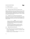
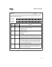
P1_PIN 1FD6H Port 1 Pin State
If you are using T1CLK (P1.4) as the clock source for the baud-rate
generator, you can read P1_PIN.4 to determine the current value of
T1CLK.
P1_REG 1FD4H Port 1 Output Data
To use T1CLK as the clock source for the baud-rate generator, set
P1_REG.4.
P2_DIR 1FCBH Port 2 Direction
This register selects the direction of each port 2 pin. Clear P2_DIR.1
to configure RXD (P2.1) as a high-impedance input/open-drain
output, and set P2_DIR.0 to configure TXD (P2.0) as a comple-
mentary output.
P2_MODE 1FC9H Port 2 Mode
This register selects either the general-purpose input/output function
or the peripheral function for each pin of port 2. Set P2_MODE.1:0
to configure TXD (P2.0) and RXD (P2.1) for the SIO port.
P2_PIN 1FCFH Port 2 Pin State
Two bits of this register contain the values of the TXD (P2.0) and
RXD (P2.1) pins. Read P2_PIN to determine the current value of the
pins.
P2_REG 1FCDH Port 2 Output Data
This register holds data to be driven out on the pins of port 2. Set
P2_REG.1 for the RXD (P2.1) pin. Write the desired output data for
the TXD (P2.0) pin to P2_REG.0.
SBUF_RX 1FB8H Serial Port Receive Buffer
This register contains data received from the serial port.
SBUF_TX 1FBAH Serial Port Transmit Buffer
This register contains data that is ready for transmission. In modes
1, 2, and 3, writing to SBUF_TX starts a transmission. In mode 0,
writing to SBUF_TX starts a transmission only if the receiver is
disabled (SP_CON.3 = 0)
SP_BAUD 1FBCH,1FBDH Serial Port Baud Rate
This register selects the serial port baud rate and clock source. The
most-significant bit selects the clock source. The lower 15 bits
represent the BAUD_VALUE, an unsigned integer that determines
the baud rate.
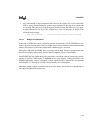
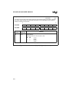
SP_CON 1FBBH Serial Port Control
This register selects the communications mode and enables or
disables the receiver, parity checking, and ninth-bit data transmis-
sions. The TB8 bit is cleared after each transmission.
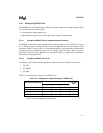
Table 8-2. Serial Port Control and Status Registers (Continued)
Mnemonic Address Description


