9-2
8XC196NP, 80C196NU USER’S MANUAL
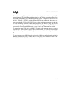
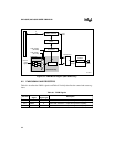
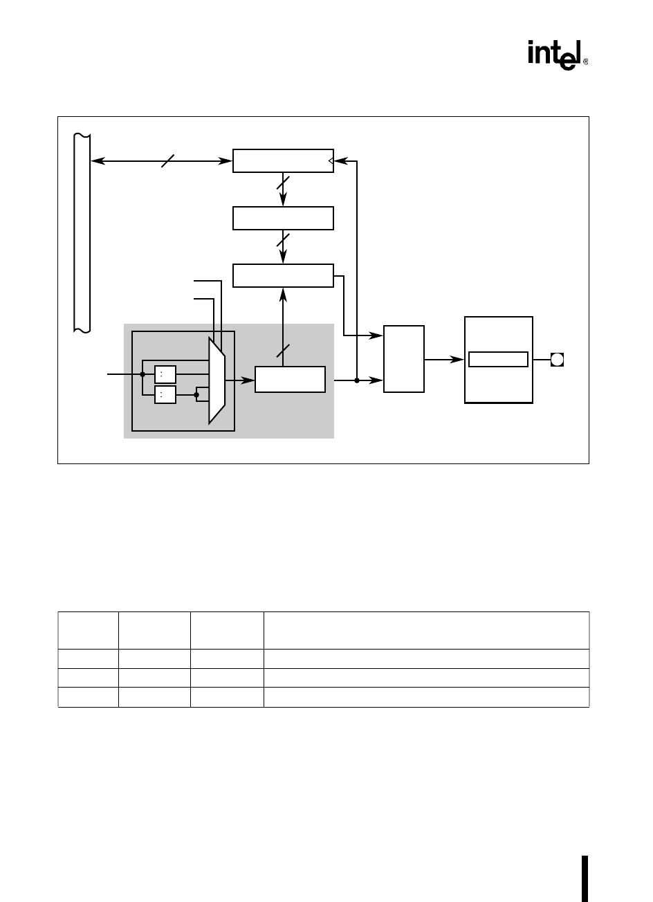
Figure 9-2. PWM Block Diagram (80C196NU Only)
9.2 PWM SIGNALS AND REGISTERS
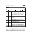
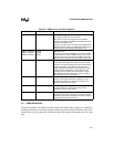
Table 9-1 describes the PWM’s signals and Table 9-2 briefly describes the control and status reg-
isters.
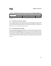
Table 9-1. PWM Signals
Port Pin
PWM
Signal
PWM
Signal Type
Description
P4.0 PWM0 O Pulse-width modulator 0 output with high-drive capability.
P4.1 PWM1 O Pulse-width modulator 1 output with high-drive capability.
P4.2 PWM2 O Pulse-width modulator 2 output with high-drive capability.
A3158-01
PWM
x
_CONTROL
R
S
Q
Port 4
Control
P4_MODE
P4.
x/
PWM
x
8
8
Buffer
x
8
Comparator
x
PWM
x
Output
Overflow
=
Load
Buffer
Internal
Clock
Signal
RS Flip-flop
x
Up Counter
– 2
00
01
10
11
Prescaler
Shared Circuitry
CON_REG0.1
(CLK1 Bit)
– 4
CON_REG0.0
(CLK0 Bit)
8


