8XC196NP, 80C196NU USER’S MANUAL
13-26
13.5.4 Comparison of Multiplexed and Demultiplexed Buses
This section compares the timings for multiplexed and demultiplexed buses. A 16-bit bus is used
for the comparison. “8-bit Bus Timings” on page 13-24 compares the 8-bit and 16-bit buses.
In a multiplexed system, where AD15:0 carry both address and data, bus activities are time-com-
pressed in comparison with a demultiplexed system, where the address and data have separate
lines (A19:0 and AD15:0). The compression is reflected in differences in specifications for the
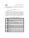
demultiplexed and multiplexed bus. Table 13-10 lists several bus specifications and their values
for demultiplexed and multiplexed buses. The data shows that the demultiplexed bus can accom-
modate slower memory devices. (See “System Bus AC Timing Specifications” on page 13-36 for
a complete list of AC timing definitons.)
13.6 WAIT STATES (READY CONTROL)
An external device can use the READY input to request wait states in addition to the wait states
that are generated internally by the 8XC196Nx device. When an address is placed on the bus for
an external bus cycle, the external device can pull the READY signal low to indicate it is not
ready. In response, the bus controller inserts wait states to lengthen the bus cycle until the external
device raises the READY signal. Each wait state adds one CLKOUT period (i.e., one state time
or 2t) to the bus cycle.
The READY signal is effective for all bus cycles, including the CCB0 fetch (which has three in-
ternal wait states). Bits WS0 and WS1 in CCB0 specify the wait states for the CCB1 fetch. There-
after, the WS0 and WS1 bits in the BUSCONx registers control the wait states, and the READY
signal can be used to insert additional wait states. (See “Controlling Wait States, Bus Width, and
Bus Multiplexing” on page 13-10.)
Table 13-10. Comparison of AC Timings for Demultiplexed and Multiplexed 16-bit Buses
Bus
Spec.
Description Demultiplexed Bus (ns)
†
Multiplexed Bus (ns)
†
T
RLDV
Max. time from RD# asserted to
valid input data on the bus.
2t – 25 t – 20
T
AVDV
Max. time from A19:0 and CS
x
#
valid to valid input data on the bus.
4t – 50 3t – 40
T
RHDZ
Max. time from RD# deasserted
until data bus is at high impedance.
tt
T
WLWH
Minimum time that WR# is
asserted.
2t – 10 t – 5
T
QVWH
Minimum time from valid data on
the bus to WR# deasserted.
3t – 33 t – 15
†
Consult the device datasheet for the latest specifications.


