8XC196NP, 80C196NU USER’S MANUAL
13-18
After RESET# is deasserted, the following pins are initialized:
• The P2.7/CLKOUT pin operates as CLKOUT (as during reset). Be sure that the CLKOUT
signal does not damage external hardware.
• The P3.0/CS0# pin operates as CS0#, which is asserted for the CCB fetches. If you plan to
use the P3.0 pin as an input, it must be reconfigured from its post-reset operation as an
output.
• The BHE#/WRH# pin operates as BHE#.
• The WR#/WRL# pin operates as WR#.
• Bus-hold function is disabled internally (WSR.7 = 0).
• The READY/P5.6 pin is active (that is, the chip responds to external requests for additional
wait states).
• The INST pin is low (deasserted).
• The AD15:0 pins are active.
• The following port pins are weakly held high: P1.7:0, P2.6, P2.4:0, P3.7:1, and P4.7:0.
• The EPORT.3:0 pins are forced high, regardless of the state of the EA# pin.
Following reset, you should set the stack pointer and initialize the chip-select outputs using the
procedure in “Example of a Chip-select Setup” on page 13-12.
13.5 BUS WIDTH AND MULTIPLEXING
The external bus can operate with a 16-bit or 8-bit data bus and with a multiplexed or demulti-
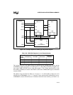
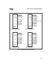
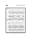
plexed address/data bus. Figure 13-8 shows the external bus signals during operation in the four
combinations of bus width and multiplexing.


