


8XC196MC, MD, MH USER’S MANUAL
C-34
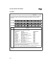
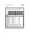
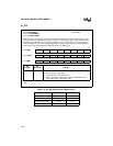
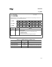
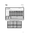
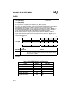
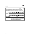
Px_REG
P
x
_REG
x
= 2–5 (8XC196MC)
x
= 2–5, 7 (8XC196MD)
x
= 1–5 (8XC196MH)
Address:
Reset State:
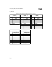
Table C-10
For an input, set the corresponding port
x
data output (P
x
_REG) register bit.
For an output, write the data to be driven out by each pin to the corresponding bit of P
x
_REG. When a
pin is configured as standard I/O (P
x
_MODE.
y
= 0), the result of a CPU write to P
x
_REG is
immediately visible on the pin. When a pin is configured as a special-function signal (P
x
_MODE.
y
= 1),
the associated on-chip peripheral or off-chip component controls the pin. The CPU can still write to
P
x
_REG, but the pin is unaffected until it is switched back to its standard I/O function.
This feature allows software to configure a pin as standard I/O (clear P
x
_MODE.
y
), initialize or
overwrite the pin value, then configure the pin as a special-function signal (set P
x
_MODE.
y
). In this
way, initialization, fault recovery, exception handling, etc., can be done without changing the operation
of the associated peripheral.
7 0
x
= 1 (MH) ————PIN3 PIN2 PIN1 PIN0
7 0
x
= 2–5 (M
x
) PIN7 PIN6 PIN5 PIN4 PIN3 PIN2 PIN1 PIN0
7 0
x
= 7 (MD) PIN7 PIN6 PIN5 PIN4 PIN3 PIN2 PIN1 PIN0
Bit Number
Bit
Mnemonic
Function
7:0
†
PIN7:0 Port
x
Pin
y
Output
To u se P
x
.
y
for output, write the desired output data to this bit. To use
P
x
.
y
for input, set this bit.
†
The bits shown as dashes (—) are reserved; for compatibility with future devices, write zeros to
these bits.
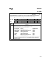
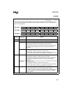
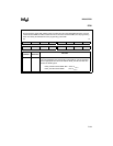
Table C-10. P
x
_REG Addresses and Reset Values
Register Address Reset Value
P1_REG (8XC196MH) 1F9DH FFH
P2_REG (8XC196M
x
) 1FD4H FFH
P3_REG (8XC196M
x
) 1FFCH FFH
P4_REG (8XC196M
x
) 1FFDH FFH
P5_REG (8XC196MC, MD)
P5_REG (8XC196MH)
1FF5H
1FF5H
FFH when pin is not driven
FFH
P7_REG (8XC196MD) 1FD5H FFH