8XC196MC, MD, MH USER’S MANUAL
15-4
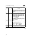
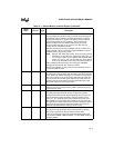
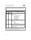
WRH# P5.5 O Write High
†
During 16-bit bus cycles, this active-low output signal is asserted for
high-byte writes and word writes to external memory. During 8-bit bus
cycles, WRH# is asserted for all write operations.
†
The chip configuration register 0 (CCR0) determines whether this
pin functions as BHE# or WRH#. CCR0.2 = 1 selects BHE#;
CCR0.2 = 0 selects WRH#.
WRL# P5.2 O Write Low
†
During 16-bit bus cycles, this active-low output signal is asserted for
low-byte writes and word writes to external memory. During 8-bit bus
cycles, WRL# is asserted for all write operations.
†
The chip configuration register 0 (CCR0) determines whether this
pin functions as WR# or WRL#. CCR0.2 = 1 selects WR#; CCR0.2 =
0 selects WRL#.
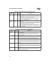
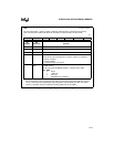
Table 15-2. External Memory Interface Registers
Register
Mnemonic
Address Description
CCR0 2018H Chip Configuration 0
Controls powerdown mode, bus-control signals, and internal memory
protection. Three of its bits combine with two bits of CCR1 to control wait
states and bus width.
CCR1 201AH Chip Configuration 1
Enables the watchdog timer and selects the bus timing mode. Two of its bits
combine with three bits of CCR0 to control wait states and bus width.
P5_DIR 1FF3H Port 5 Direction
Each bit of P5_DIR controls the direction of the corresponding pin. Clearing
a bit configures a pin as a complementary output; setting a bit configures a
pin as an input or open-drain output. (Open-drain outputs require external
pull-ups.)
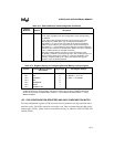
P5_MODE 1FF1H Port 5 Mode
Each bit of P5_MODE controls whether the corresponding pin functions as a
standard I/O port pin or as a special-function signal. Setting a bit configures a
pin as a special-function signal; clearing a bit configures a pin as a standard
I/O port pin.
P5_PIN 1FF7H Port 5 Input
Each bit of P5_PIN reflects the current state of the corresponding pin,
regardless of the pin configuration.
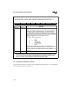
Table 15-1. External Memory Interface Signals (Continued)
Signal
Name
Port Pin Type Description


