


6-7
I/O PORTS
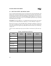
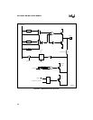
In I/O mode (selected by clearing Px_MODE.y), Px_REG and Px_DIR are input to the multiplex-
ers. These signals combine to drive the gates of Q1 and Q2 so that the output is high, low, or high
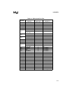
impedance. Table 6-6 is a logic table for I/O operation of these ports.
In special-function mode (selected by setting Px_MODE.y), SFDIR and SFDATA are input to the
multiplexers. These signals combine to drive the gates of Q1 and Q2 so that the output is high,
low, or high impedance. Special-function output signals clear SFDIR; special-function input sig-
nals set SFDIR. Table 6-7 is a logic table for special-function operation of these ports. Even if a
pin is to be used in special-function mode, you must still initialize the pin as an input or output
by writing to Px_DIR.
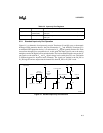
Resistor R1 provides ESD protection for the pin. Input signals are buffered. The standard ports
use Schmitt-triggered buffers for improved noise immunity. Port 5 uses a standard input buffer
because of the high speeds required for bus control functions. The signals are latched into the
Px_PIN sample latch and output onto the internal bus when the Px_PIN register is read.
The falling edge of RESET# turns on transistor Q3, which remains on for about 300 ns, causing
the pin to change rapidly to its reset state. The active-low level of RESET# turns on transistor Q4,
which weakly holds the pin high. (Q4 can source approximately –10 µA; consult the datasheet
for exact specifications.) Q4 remains on, weakly holding the pin high, until your software writes
to the Px_MODE register.
NOTE (8XC196MC, MD Only)
P2.7 is an exception. After reset, P2.7 carries the CLKOUT signal (half the
crystal input frequency) rather than being held high. When CLKOUT is
selected, it is always a complementary output.