16-31
PROGRAMMING THE NONVOLATILE MEMORY
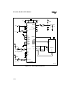
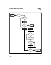
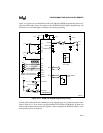
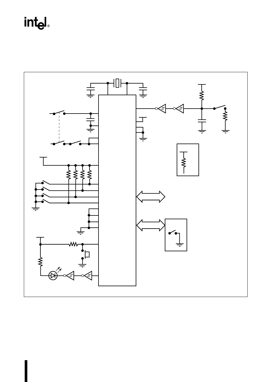
Figure 16-14 shows the recommended circuit for PCCB and UPROM programming. In these cir-
cuits, the PBUS holds data to be written to the OTPROM, PALE# begins programming, and
PVER drives an LED that lights to indicate successful programming.
Figure 16-14. PCCB and UPROM Programming Circuit
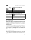
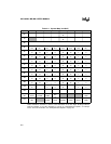
To enter either mode, follow the standard power-up sequence (page 16-14) after setting the values
listed in Table 16-13. If you want to program both the PCCB and the UPROM bits, program one
of them and complete the power-down sequence. Then reconfigure the PMODE and port 3 pins
and repeat the power-up sequence.
+5.0V
XTAL1
20 pF
20 pF
XTAL2
P2.1/PALE#
P2.0/PVER
RESET#
+12.50V
100 kΩ
1 kΩ
10µF
74HC14
1.0µF
Reset
EA#
V
PP
V
REF
P0.7
P0.6
P0.5
P0.4
P0.3:0
P1.4:0
P2.5:2
ANGND
READY/P5.6
NMI
BUSWIDTH/P5.7
87C196 Device
V
CC
A3003-02
V
CC
V
CC
V
SS
270kΩ
V
CC
74HC14
Push to Program
10kΩ
10kΩ
V
CC
Pullups Required
P4.7 – P3.0
V
CC
SW1
PMODE = 0DH PCCB Mode
PMODE = 09H UPROM Mode
P3.7:0
PCCB/UPROM
Value
SW2
P4.7:0


