


B-23
SIGNAL DESCRIPTIONS
8XC196MD. Table B-9 lists the same information for the 8XC196MH. Table B-7 defines the
symbols used to represent the pin status. Refer to the DC Characteristics table in the datasheet for
actual specifications for V
OL
, V
IL
, V
OH
, and V
IH
.
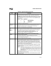
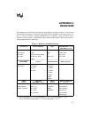
Table B-7. Definition of Status Symbols
Symbol Definition Symbol Definition
0 Voltage less than or equal to V
OL
, V
IL
MD0 Medium pull-down
1 Voltage greater than or equal to V
OH
, V
IH
MD1 Medium pull-up
HiZ High impedance WK0 Weak pull-down
LoZ0 Low impedance; strongly driven low WK1 Weak pull-up
LoZ1 Low impedance; strongly driven high ODIO Open-drain I/O
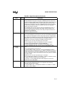
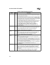
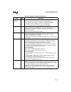
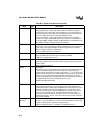
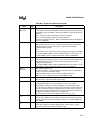
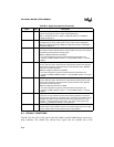
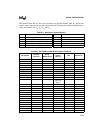
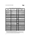
Table B-8. 8XC196MC and MD Default Signal Conditions
Port Signals
Alternate
Functions
During
RESET# Active
Upon RESET#
Inactive
(Note 14)
Idle Powerdown
P0.7:0 ACH7:0 HiZ — HiZ HiZ
P1.1:0 ACH9:8 HiZ — HiZ HiZ
P1.2 ACH10/T1CLK HiZ — HiZ HiZ
P1.3 ACH11/T1DIR HiZ — HiZ HiZ
P1.4 ACH12 HiZ — HiZ HiZ
P1.5 (Note 15) ACH13 HiZ — HiZ HiZ
P1.7:6 (Note 15) — HiZ — HiZ HiZ
P2.0 EPA0 WK1 (Note 1) WK1 (Note 12) (Note 12)
P2.1 EPA1 WK1 WK1 (Note 12) (Note 12)
P2.3:2 EPA3:2 WK1 WK1 (Note 12) (Note 12)
P2.6:4 COMP2:0 WK1 WK1; except
P2.5 = LZ
(Note 1)
(Note 12) (Note 12)
P2.7 COMP3 WK1 WK1 (Note 12) (Note 12)
P3.7:0 AD7:0 WK1 HiZ (Note 3) (Note 3)
P4.7:0 AD15:8 WK1 HiZ (Note 3) (Note 3)
P5.0 ADV#/ALE WK1 (Note 1) WK1 (Note 4) (Note 8) (Note 8)
P5.1 INST WK1 WK1 (Note 9) (Note 9)
P5.2 WR#/WRL# WK1 (Note 1) WK1 (Note 10) (Note 10)
P5.3 RD# WK1 (Note 1) WK1 (Note 4) (Note 10) (Note 10)
P5.4 ONCE# MD1 LZ (Note 1) (Note 10) (Note 10)
P5.5 BHE#/WRH# WK1 WK1 (Note 4) (Note 10) (Note 10)
P5.6 READY WK1 (Note 5) (Note 11) (Note 11)
P5.7 BUSWIDTH WK1 (Note 6) (Note 11) (Note 11)
P6.0 WG1# WK1 WK1 (Note 13) (Note 13)
P6.1 WG1 WK1 WK1 (Note 13) (Note 13)
P6.2 WG2# WK1 WK1 (Note 13) (Note 13)