12-5
ANALOG-TO-DIGITAL (A/D) CONVERTER
12.4.1 Programming the A/D Test Register
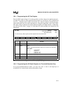
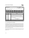
The AD_TEST register (Figure 12-2) analog specifies an offset voltage to be applied to the resis-
tor ladder. To use the zero-offset adjustment, first perform two conversions, one on ANGND and
one on V
REF
. With the results of these conversions, use a software routine to calculate the zero-
offset error. Specify the zero-offset adjustment by writing the appropriate value to AD_TEST.
This offset voltage is added to the resistor ladder and applies to all input channels. “Understand-
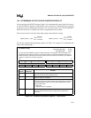
ing A/D Conversion Errors” on page 12-13 describes zero-offset and other errors inherent in A/D
conversions.
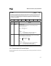
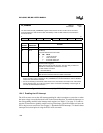
12.4.2 Programming the A/D Result Register (for Threshold Detection Only)
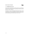
To use the threshold-detection modes, you must first write a value to the high byte of
AD_RESULT to set the desired reference (threshold) voltage.
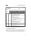
AD_TEST
Address:
Reset State (MC, MD):
Reset State (MH):
1FAEH
C0H
88H
The A/D test (AD_TEST) register specifies adjustments for DC offset errors.
7 0
— — — OFF1 — OFF0 — —
Bit
Number
Bit
Mnemonic
Function
7:5 — Reserved; for compatibility with future devices, write zeros to these bits.
4 OFF1 Offset
This bit , along with OFF0 (bit 2) allows you to set the zero offset point.
OFF1 OFF0
00 no adjustment
0 1 add 2.5 mV
1 0 subtract 2.5 mV
1 1 subtract 5.0 mV
3 — Reserved; for compatibility with future devices, write zero to this bit.
2 OFF0 See bit 4 (OFF1).
1:0 — Reserved; for compatibility with future devices, write zeros to these bits.
Figure 12-2. A/D Test (AD_TEST) Register


