


6-3
I/O PORTS
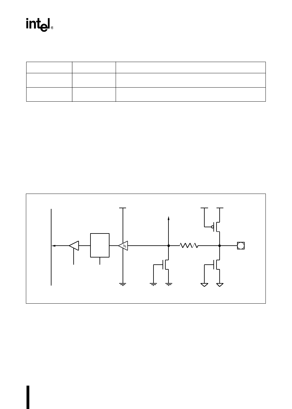
6.2.1 Standard Input-only Port Operation
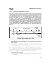
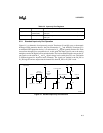
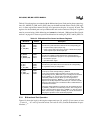
Figure 6-1 is a schematic of an input-only port pin. Transistors Q1 and Q2 serve as electrostatic
discharge (ESD) protection devices; they are referenced to V
REF
and ANGND. Transistor Q3 is
an additional ESD protection device; it is referenced to V
SS
(digital ground). Resistor R1 limits
current flow through Q3 to acceptable levels. At this point, the input signal is sent to the analog
multiplexer and to the digital level-translation buffer. The level-translation buffer converts the in-
put signals to work with the V
CC
and V
SS
digital voltage levels used by the CPU core. This buffer
is Schmitt-triggered for improved noise immunity. The signals are latched in the P0_PIN or
P1_PIN register and are output onto the internal bus when P0_PIN or P1_PIN is read.
Figure 6-1. Standard Input-only Port Structure
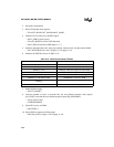
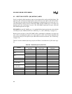
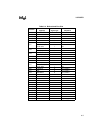
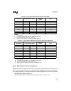
Table 6-3. Input-only Port Registers
Mnemonic Address Description
P0_PIN 1FA8H (MC, MD)
1FDAH (MH)
Each bit of P0_PIN reflects the current state of the corresponding
port 0 pin.
P1_PIN (MC, MD) 1FA9H (MC, MD) Each bit of P1_PIN reflects the current state of the corresponding
port 1 pin.
V
REF
Q3
Q1
Level
Translation
Buffer
PH1 Clock
PORT 0
Data Register
Internal Bus
P0_PIN
DQ
V
REF
Vss
150 to 200 Ohms
Q2
ANGNDANGND
To Analog MUX
Vss
Vss
Vcc
Buffer
Read Port
R1
LE
Input Pin
A0236-01