


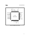
B-15
SIGNAL DESCRIPTIONS
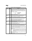
BUSWIDTH I Bus Width
Two chip configuration register bits, CCR0.1 and CCR1.2, along with the
BUSWIDTH pin, control the data bus width. When both CCR bits are set, the
BUSWIDTH signal selects the external data bus width. When only one CCR bit
is set, the bus width is fixed at either 16 or 8 bits, and the BUSWIDTH signal
has no effect.
CCR0.1 CCR1.2 BUSWIDTH
0 1 X fixed 8-bit data bus
1 0 X fixed 16-bit data bus
1 1 high 16-bit data bus
1 1 low 8-bit data bus
BUSWIDTH is multiplexed with P5.7.
CLKOUT
(MC, MD)
O Clock Output
Output of the internal clock generator. The CLKOUT frequency is ½ the
oscillator input frequency (F
XTAL1
). CLKOUT has a 50% duty cycle.
CLKOUT is not implemented on the 8XC196MH.
COMP3:0 (MC,
MH)
COMP5:0
(MD)
O Event Processor Array (EPA) Compare Pins
These signals are the output of the EPA compare-only channels. These pins
are multiplexed with other signals and may be configured as standard I/O.
COMP5:0 are multiplexed as follows: COMP0/P2.4/AINC#,
COMP1/P2.5/PACT#, COMP2/P2.6/CPVER, COMP3/P2.7(MC, MD),
COMP3/P2.3 (MH), COMP4/P7.2, and COMP5/P7.3.
COMP4 and COMP5 are not implemented on the 8XC196MC and MH.
CPVER O Cumulative Program Verification
During slave programming, a high signal indicates that all locations
programmed correctly, while a low signal indicates that an error occurred during
one of the programming operations.
CPVER is multiplexed with P2.6 and COMP2.
EA# I External Access
This input determines whether memory accesses to special-purpose and
program memory partitions are directed to internal or external memory. (See
Table 4-1 on page 4-2 for address ranges of special-purpose and program
memory partitions.) These accesses are directed to internal memory if EA# is
held high and to external memory if EA# is held low. For an access to any other
memory location, the value of EA# is irrelevant.
EA# also controls entry into the programming modes. If EA# is at V
PP
voltage
(typically +12.5 V) on the rising edge of RESET#, the microcontroller enters a
programming mode.
NOTE: Systems with EA# tied inactive have idle time between external bus
cycles. When the address/data bus is idle, you can use ports 3 and 4
for I/O. Systems with EA# tied active cannot use ports 3 and 4 as
standard I/O; when EA# is active, these ports will function only as the
address/data bus.
EA# is sampled and latched only on the rising edge of RESET#. Changing the
level of EA# after reset has no effect.
Always connect EA# to V
SS
when using a microcontroller that has no internal
nonvolatile memory.
Table B-6. Signal Descriptions (Continued)
Name Type Description