8XC196MC, MD, MH USER’S MANUAL
15-14
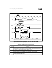
15.3.2 16-bit Bus Timings
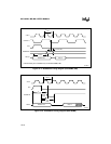
When the microcontroller is configured to operate in the 16-bit bus-width mode, lines AD15:0
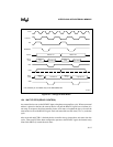
form a 16-bit multiplexed address/data bus. Figure 15-6 shows an idealized timing diagram for
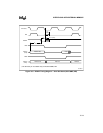
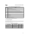
the external read and write cycles. Comprehensive timing specifications are shown in Figure
15-22 on page 15-32.
The rising edge of the address latch enable (ALE) signal indicates that the microcontroller is driv-
ing an address onto the bus (AD15:0). The microcontroller presents a valid address before ALE
falls. The ALE signal is used to strobe a transparent latch (such as a 74AC373), which captures
the address from AD15:0 and holds it while the bus controller puts data onto AD15:0.
For 16-bit read cycles, the bus controller floats the bus and then drives RD# low so that it can
receive data. The external memory must put data (Data In) onto the bus before the rising edge of
RD#. The datasheet specifies the maximum time the memory device has to output valid data after
RD# is asserted (T
RLDV
). When INST is asserted, it indicates that the read operation is an instruc-
tion fetch.
For 16-bit write cycles, the bus controller drives WR# low, then puts data onto the bus. The rising
edge of WR# signifies that data is valid. At this time, the external system must latch the data.


