


8XC196MC, MD, MH USER’S MANUAL
6-6
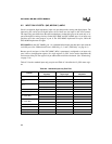
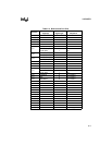
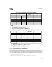
Table 6-5 lists the registers associated with the bidirectional ports. Each port has three control reg-
isters (Px_MODE, Px_DIR, and Px_REG); they can be both read and written. The Px_PIN regis-
ter is a status register that returns the logic level present on the pins; it can only be read. The
registers for the standard ports are byte-addressable and can be windowed. The port 5 registers
must be accessed using 16-bit addressing and cannot be windowed. “Bidirectional Port Consid-
erations” on page 6-12 discusses special considerations for reading P2_REG.7 and P6_REG.7:4.
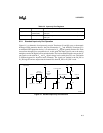
6.3.1 Bidirectional Port Operation
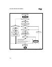
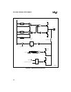
Figure 6-2 shows the logic for driving the output transistors, Q1 and Q2. Q1
can source at least
–3 mA at V
CC
– 0.7 volts. Q2 can sink at least 3 mA at 0.45 volts. (Consult the datasheet for spec-
ifications.)
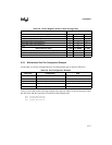
Table 6-5. Bidirectional Port Control and Status Registers
Mnemonic Address Description
P1_DIR (MH)
P2_DIR
P5_DIR
P7_DIR (MD)
1F9BH
1FD2H
1FF3H
1FD3H
Port
x
Direction
Each bit of P
x
_DIR controls the direction of the corresponding pin.
0 = complementary output (output only)
1 = input or open-drain output (input, output, or bidirectional) Open-
drain outputs require external pull-ups.
P1_MODE (MH)
P2_MODE
P5_MODE
P7_MODE (MD)
1F99H
1FD0H
1FF1H
1FD1H
Port
x
Mode
Each bit of P
x
_MODE controls whether the corresponding pin
functions as a standard I/O port pin or as a special-function signal.
0 = standard I/O port pin
1 = special-function signal
P1_PIN (MH)
P2_PIN
P5_PIN
P7_PIN (MD)
1F9FH
1FD6H
1FF7H
1FD7H
Port
x
Input
Each bit of P
x
_PIN reflects the current state of the corresponding
pin, regardless of the pin configuration.
P1_REG (MH)
P2_REG
P5_REG
P7_REG (MD)
1F9DH
1FD4H
1FF5H
1FD5H
Port
x
Data Output
For an input, set the corresponding P
x
_REG bit.
For an output, write the data to be driven out by each pin to the
corresponding bit of P
x
_REG. When a pin is configured as standard
I/O (P
x
_MODE.
y
= 0), the result of a CPU write to P
x
_REG is
immediately visible on the pin. When a pin is configured as a
special-function signal (P
x
_MODE.
y
= 1), the associated on-chip
peripheral or off-chip component controls the pin. The CPU can still
write to P
x
_REG, but the pin is unaffected until it is switched back to
its standard I/O function.
This feature allows software to configure a pin as standard I/O (clear
P
x
_MODE.
y
), initialize or overwrite the pin value, then configure the
pin as a special-function signal (set P
x
_MODE.
y
). In this way, initial-
ization, fault recovery, exception handling, etc., can be done without
changing the operation of the associated peripheral.