


12-11
ANALOG-TO-DIGITAL (A/D) CONVERTER
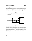
Typically, the (R
F
/ A
V
+ 1) term is the major contributor to the total resistance and the factor that
determines the minimum sample time specified in the datasheet.
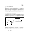
12.6.1.1 Minimizing the Effect of High Input Source Resistance
Under some conditions, the input source resistance (R
SOURCE
) can be great enough to affect the
measurement. You can minimize this effect by increasing the sample time or by connecting an
external capacitor (C
EXT
) from the input pin to ANGND. The external signal will charge C
EXT
to
the source voltage level. When the channel is sampled, C
EXT
acts as a low-impedance source to
charge the sample capacitor (C
S
). A small portion of the charge in C
EXT
is transferred to C
S
, re-
sulting in a drop of the sampled voltage. The voltage drop is calculated using the following for-
mula.
If C
EXT
is 0.005 µF or greater, the error will be less than –0.4 LSB in 10-bit conversion mode. The
use of C
EXT
in conjunction with R
SOURCE
forms a low-pass filter that reduces noise input to the
A/D converter.
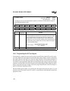
High R
SOURCE
resistance can also cause errors due to the input leakage (I
LI
1
). I
LI
1
is typically much
lower than its specified maximum (consult the datasheet for specifications). The combined effect
of I
LI
1
leakage and high R
SOURCE
resistance is calculated using the following formula.
where:
R
SOURCE
is the input source resistance, in ohms
I
LI
1
is the input leakage, in amperes
V
REF
is the reference voltage, in volts
External circuits with R
SOURCE
resistance of 1 kilo-ohm or lower and V
REF
equal to 5.0 volts will
have a resultant error due to source impedance of 0.6 LSB or less.
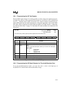
Sampled Voltage Drop, %
C
S
C
EXT
C
S
+
---------------------------
100%×=
error (LSBs)
R
SOURCE
I
LI1
× 1024×
V
REF
------------------------------------------------------------
=