8XC196MC, MD, MH USER’S MANUAL
6-14
6.4 BIDIRECTIONAL PORTS 3 AND 4 (ADDRESS/DATA BUS)
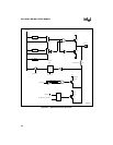
Ports 3 and 4 are eight-bit, bidirectional, memory-mapped I/O ports. They can be addressed only
with indirect or indexed addressing and cannot be windowed. Ports 3 and 4 provide the multi-
plexed address/data bus. In programming modes, ports 3 and 4 serve as the programming bus
(PBUS). Port 5 supplies the bus-control signals.
During external memory bus cycles, the processor takes control of ports 3 and 4 and automatical-
ly configures them as complementary output ports for driving address/data or as inputs for read-
ing data. For this reason, these ports have no mode registers.
Systems with EA# tied inactive have idle time between external bus cycles. When the address/da-
ta bus is idle, you can use the ports for I/O. Like port 5, these ports use standard CMOS input
buffers. However, ports 3 and 4 must be configured entirely as complementary or open-drain
ports; their pins cannot be configured individually. Systems with EA# tied active cannot use ports
3 and 4 as standard I/O; when EA# is active, these ports will function only as the address/data bus.
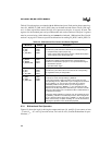
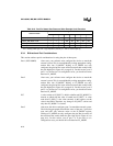
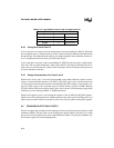
Table 6-11 lists the port 3 and 4 pins with their special-function signals and associated peripher-
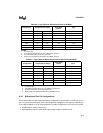
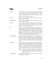
als. Table 6-12 lists the registers that affect the function and indicate the status of ports 3 and 4.
Table 6-11. Ports 3 and 4 Pins
Port Pins
Special-function
Signal(s)
Special-function
Signal Type
Associated Peripheral
P3.7:0
AD7:0 I/O Address/data bus, low byte
PBUS7:0 I/O Programming bus, low byte
P4.7:0
AD15:8 I/O Address/data bus, high byte
PBUS15:8 I/O Programming bus, high byte
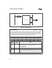
Table 6-12. Ports 3 and 4 Control and Status Registers
Mnemonic Address Description
P3_PIN
P4_PIN
1FFEH
1FFFH
Port
x
Input
Each bit of P
x
_PIN reflects the current state of the corresponding pin,
regardless of the pin configuration.
P3_REG
P4_REG
1FFCH
1FFDH
Port
x
Data Output
Each bit of P
x
_REG contains data to be driven out by the corresponding
pin.
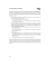
When the device requires access to external memory, it takes control of
the port and drives the address/data bit onto the pin. The address/data
bit replaces your output during this time. When the external access is
completed, the device restores your data onto the pin.


