B-17
SIGNAL DESCRIPTIONS
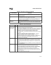
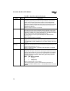
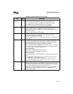
ONCE# I On-circuit Emulation
Holding ONCE# low during the rising edge of RESET# places the device into
on-circuit emulation (ONCE) mode. This mode puts all pins, except XTAL1 and
XTAL2, into a high-impedance state, thereby isolating the device from other
components in the system. The value of ONCE# is latched when the RESET#
pin goes inactive. While the device is in ONCE mode, you can debug the
system using a clip-on emulator.
To exit ONCE mode, reset the device by pulling the RESET# signal low. To
prevent inadvertent entry into ONCE mode, either configure this pin as an
output or hold it high during reset and ensure that your system meets the V
IH
specification (see datasheet).
ONCE# is multiplexed with P5.4.
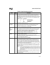
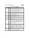
P0.7:0 I Port 0
This is a high-impedance, input-only port. Port 0 pins should not be left floating.
These pins may individually be used as analog inputs (ACH
x
) or digital inputs
(P0.
y
). While it is possible for the pins to function simultaneously as analog and
digital inputs, this is not recommended because reading port 0 while a
conversion is in process can produce unreliable conversion results.
ANGND and V
REF
must be connected for port 0 to function.
Port 0 is multiplexed as follows: P0.0/ACH0, P0.1/ACH1, P0.2/ACH2,
P0.3/ACH3, P0.4/ACH4/PMODE.0, P0.5/ACH5/PMODE.1,
P0.6/ACH6/PMODE.2 (MC, MD), P0.6/ACH6/T1CLK/PMODE.2 (MH),
P0.7/ACH7/PMODE.3 (MC, MD), and P0.7/ACH7/T1DIR/PMODE.3 (MH).
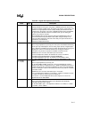
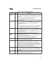
P1.4:0 (MC)
P1.7:0 (MD)
I Port 1
This is a high-impedance, input-only port.
On the 8XC196MC and MD, some port 1 pins may individually be used as
analog inputs (ACH
x
) or digital inputs (P1.
y
). While it is possible for the pins to
function simultaneously as analog and digital inputs, this is not recommended
because reading port 1 while a conversion is in process can produce unreliable
conversion results.
ANGND and V
REF
must be connected for port 1 to function.
Port 1 is multiplexed as follows: P1.0/ ACH8, P1.1/ACH9, P1.2/ACH10/T1CLK,
P1.3/ACH11/T1DIR, P1.4/ACH12, and P1.5/ACH13).
P1.6 and P1.7 are not multiplexed with any other signals. P1.7:5 are not
implemented on the 8XC196MC.
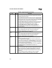
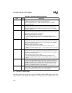
P1.3:0 (MH) I/O Port 1
This is a standard, bidirectional port that is multiplexed with individually
selectable special-function signals.
On the 8XC196MH, port 1 is multiplexed as follows: P1.0/ TXD0, P1.1/RXD0,
P1.2/TXD1, and P1.3/RXD1.
Table B-6. Signal Descriptions (Continued)
Name Type Description


