


C-11
REGISTERS
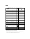
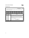
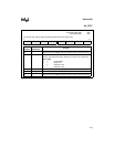
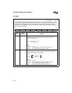
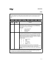
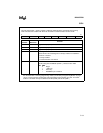
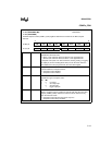
CCR0
CCR0
no direct access†
The chip configuration 0 (CCR0) register controls powerdown mode, bus-control signals, and internal
memory protection. Three of its bits combine with two bits of CCR1 to control wait states and bus
width.
7 0
LOC1 LOC0 IRC1 IRC0 ALE WR BW0 PD
Bit
Number
Bit
Mnemonic
Function
7:6 LOC1:0 Lock Bits
These two bits control read and write access to the OTPROM during
normal operation. Refer to “Controlling Access to the OTPROM During
Normal Operation” on page 16-4 for details.
LOC1 LOC0
0 0 read and write protect
0 1 read protect only
1 0 write protect only
1 1 no protection
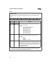
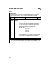
5:4 IRC1:0 Internal Ready Control
These two bits, along with IRC2 (CCR1.1) and the READY pin determine
the number of wait states that can be inserted into the bus cycle. While
READY is held low, wait states are inserted into the bus cycle until the
programmed number of wait states is reached. If READY is pulled high
before the programmed number of wait states is reached, no additional
wait states will be inserted into the bus cycle.
IRC2 IRC1 IRC0
0 0 0 zero wait states
0X1illegal
11Xillegal
100one wait state
1 0 1 two wait states
110three wait states
111infinite
If you choose the infinite wait states option, you must keep P5.6
configured as the READY signal. Also, be sure to add external hardware
to count wait states and pull READY high within a specified time.
Otherwise, a defective external device could tie up the address/data bus
indefinitely.
†
The CCRs are loaded with the contents of the chip configuration bytes (CCBs) after reset, unless the
microcontroller is entering programming modes (see “Entering Programming Modes” on page 16-13),
in which case the programming chip configuration bytes (PCCBs) are used. The CCBs reside in
nonvolatile memory at addresses 2018H (CCB0) and 201AH (CCB1).