15-21
INTERFACING WITH EXTERNAL MEMORY
15.5 BUS-CONTROL MODES
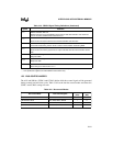
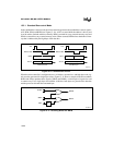
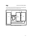
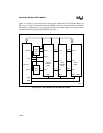
The ALE and WR bits (CCR0.3 and CCR0.2) define which bus-control signals will be generated
during external read and write cycles. Table 15-6 lists the four bus-control modes and shows the
CCR0.3 and CCR0.2 settings for each.
.
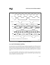
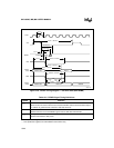
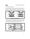
T
LLYX
††
READY Hold after ALE Low
Minimum time the level of the READY signal must be valid after ALE falls. If the maximum
value is exceeded, additional wait states will occur.
T
LLYV
††
ALE Low to READY Setup
Maximum time the external device has to deassert READY after ALE falls.
T
QVWH
Data Valid to WR# High
Time between data being valid on the bus and the microcontroller deasserting WR#.
T
RLDV
RD# Low to Input Data Valid
Maximum time the memory system has to output valid data after the microcontroller asserts
RD#.
T
RLRH
RD# Low to RD# High
RD# pulse width.
T
WLWH
WR# Low to WR# High
WR# pulse width.
T
XTAL1
1/F
XTAL1
All AC timings are referenced to T
XTAL1
.
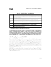
Table 15-6. Bus-control Modes
Bus-control Mode Bus-control Signals
CCR0.3
(ALE)
CCR0.2
(WR)
Standard Bus-control Mode ALE, RD#, WR#, BHE# 1 1
Write Strobe Mode ALE, RD#, WRL#, WRH# 1 0
Address Valid Strobe Mode ADV#, RD#, WR#, BHE# 0 1
Address Valid with Write Strobe Mode ADV#, RD#, WRL#, WRH# 0 0
Table 15-5. READY Signal Timing Definitions (Continued)
Symbol Definition
†
This specification applies to the 8XC196MC, MD microcontrollers only.
††
This specification applies to the 8XC196MH microcontroller only.


