16-3
PROGRAMMING THE NONVOLATILE MEMORY
16.3 SECURITY FEATURES
Several security features enable you to control access to both internal and external memory. Read
and write protection bits in the chip configuration register (CCR0), combined with a security key,
allow various levels of internal memory protection. Two UPROM bits disable fetches of instruc-
tions and data from external memory. (See Figure 16-1 on page 16-7 for more information.)
16.3.1 Controlling Access to Internal Memory
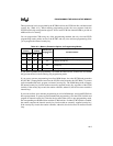
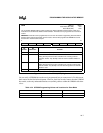
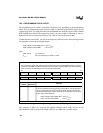
The lock bits in the chip configuration register (CCR0) control access to the OTPROM. The reset
sequence loads the CCRs from the CCBs for normal operation and from the PCCBs when enter-
ing programming modes. You can program the CCBs using any of the programming methods, but
only slave and PCCB programming modes allow you to program the PCCBs.
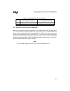
NOTE
The developers have made a substantial effort to provide an adequate program
protection scheme. However, Intel cannot and does not guarantee that these
protection methods will always prevent unauthorized access.
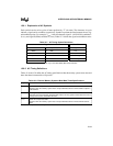
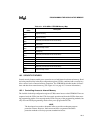
Table 16-1. 87C196M
x
OTPROM Memory Map
Address Range
(Hex)
Description
9FFF (MH)
2080
Program memory
5FFF (MC, MD)
2080
Program memory
207F
205E
Reserved (each location must contain FFH)
205D
2040
PTS vectors
203F
2030
Upper interrupt vectors
202F
2020
Security key
201F
201C
Reserved (each location must contain FFH)
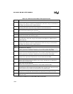
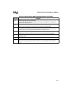
201B Reserved (must contain 20H)
201A CCB1
2019 Reserved (must contain 20H)
2018 CCB0
2017
2014
Reserved (each location must contain FFH)
2013
2000
Lower interrupt vectors


