8XC196MC, MD, MH USER’S MANUAL
12-12
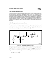
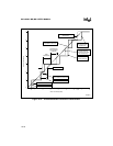
12.6.1.2 Suggested A/D Input Circuit
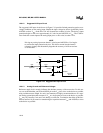
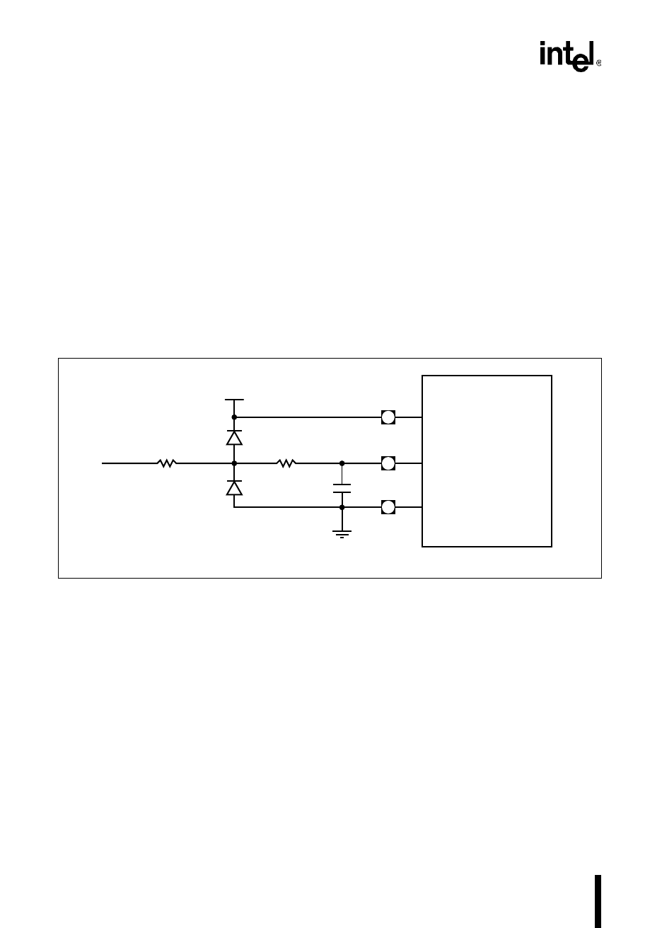
The suggested A/D input circuit shown in Figure 12-8 provides limited protection against over-
voltage conditions on the analog input. Should the input voltage be driven significantly below
ANGND or above V
REF
, diode D2 or D1 will forward bias at about 0.8 volts. The device’s input
protection begins to turn on at approximately 0.5 volts beyond ANGND or V
REF
. The 270Ω re-
sistor limits the current input to the analog input pin to a safe value, less than 1 mA.
NOTE
Driving any analog input more than 0.5 volts beyond ANGND or V
REF
begins
to activate the input protection devices. This drives current into the internal
reference circuitry and substantially degrades the accuracy of A/D conversions
on all channels.
Figure 12-8. Suggested A/D Input Circuit
12.6.1.3 Analog Ground and Reference Voltages
Reference supply levels strongly influence the absolute accuracy of the conversion. For this rea-
son, we recommend that you tie the ANGND pin to the V
SS
pin as close to the device as possible,
using a minimum trace length. In a noisy environment, we highly recommend the use of a sepa-
rate analog ground plane that connects to V
SS
at a single point as close to the device as possible.
I
REF
may vary between 2 mA and 5 mA during a conversion. To minimize the effect of this fluc-
tuation, mount a 1.0 µF ceramic or tantalum bypass capacitor between V
REF
and ANGND, as close
to the device as possible.
ACH
x
ANGND
(Optional)
D1
D2
270Ω
100Ω
0.005µF
ANGND
A0082-03
V
REF
V
REF
8XC196
Device


