


8XC196MC, MD, MH USER’S MANUAL
14-2
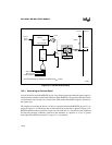
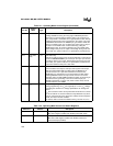
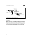
P5.4 ONCE# I On-circuit Emulation
Holding ONCE# low during the rising edge of RESET# places the
device into on-circuit emulation (ONCE) mode. This mode puts all
pins, except XTAL1 and XTAL2, into a high-impedance state, thereby
isolating the device from other components in the system. The value
of ONCE# is latched when the RESET# pin goes inactive. While the
device is in ONCE mode, you can debug the system using a clip-on
emulator. To exit ONCE mode, reset the device by pulling the
RESET# signal low. To prevent inadvertent entry into ONCE mode,
either configure this pin as an output or hold it high during reset and
ensure that your system meets the V
IH
specification (see datasheet).
P2.6 Test-mode
entry
I/O Test-mode entry
If this pin is held low during reset, the device will enter a reserved test
mode, so exercise caution if you use this pin for input. If you choose
to configure this pin as an input, always hold it high during reset and
ensure that your system meets the V
IH
specification (see datasheet)
to prevent inadvertent entry into a test mode.
— RESET# I/O Reset
A level-sensitive reset input to and open-drain system reset output
from the microcontroller. Either a falling edge on RESET# or an
internal reset turns on a pull-down transistor connected to the
RESET# pin for 16 state times. In the powerdown and idle modes,
asserting RESET# causes the chip to reset and return to normal
operating mode. The 8XC196MH provides the option of preventing an
internal reset from generating a reset on the external pin (see
“Resetting the Device” on page 13-8). After a device reset, the first
instruction fetch is from 2080H.
—V
PP
PWR Programming Voltage
During programming, the V
PP
pin is typically at +12.5 V (V
PP
voltage).
Exceeding the maximum V
PP
voltage specification can damage the
device.
V
PP
also causes the device to exit powerdown mode when it is driven
low for at least 50 ns. Use this method to exit powerdown only when
using an external clock source because it enables the internal phase
clocks, but not the internal oscillator.
On devices with no internal nonvolatile memory, connect V
PP
to V
CC
.
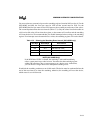
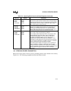
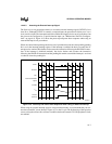
Table 14-2. Operating Mode Control and Status Registers
Mnemonic Address Description
CCR0 2018H Chip Configuration 0 Register
Bit 0 of this register enables and disables powerdown mode.
INT_MASK1 0013H Interrupt Mask 1
Bit 6 of this 8-bit register enables and disables (masks) the
external interrupt (EXTINT).
Table 14-1. Operating Mode Control Signals (Continued)
Port Pin
Signal
Name
Type Description