


8XC196MC, MD, MH USER’S MANUAL
B-22
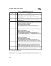
B.4 DEFAULT CONDITIONS
Table B-8 lists the values of the signals of the 8XC196MC and 8XC196MD during various oper-
ating conditions. The shaded rows indicate those signals that are available only on the
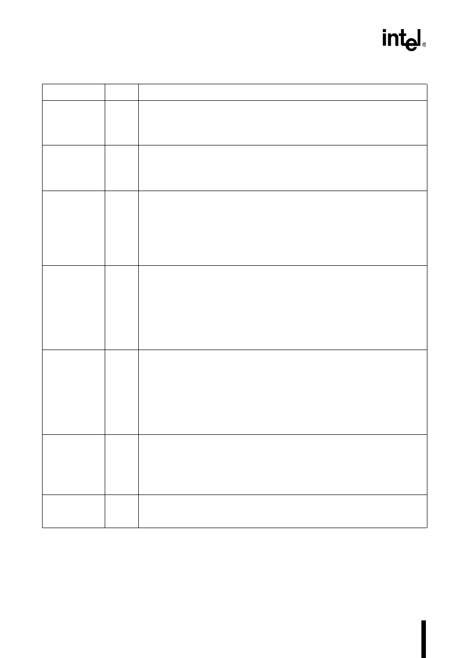
WG3:1 O Waveform Generator Phase 1–3 Positive Outputs
3-phase output signals used in motion-control applications.
WG1 is multiplexed with P6.1, WG2 is multiplexed with P6.3, and WG3 is
multiplexed with P6.5.
WG3:1# O Waveform Generator Phase 1–3 Negative Outputs
Complimentary 3-phase output signals used in motion-control applications.
WG1# is multiplexed with P6.0, WG2# is multiplexed with P6.2, and WG3# is
multiplexed with P6.4.
WR# O Write
†
This active-low output indicates that an external write is occurring. This signal is
asserted only during external memory writes.
WR# is multiplexed with P5.2 and WRL#.
†
The chip configuration register 0 (CCR0) determines whether this pin
functions as WR# or WRL#. CCR0.2 = 1 selects WR#; CCR0.2 = 0 selects
WRL#.
WRH# O Write High
†
During 16-bit bus cycles, this active-low output signal is asserted for high-byte
writes and word writes to external memory. During 8-bit bus cycles, WRH# is
asserted for all write operations.
WRH# is multiplexed with P5.5 and BHE#.
†
The chip configuration register 0 (CCR0) determines whether this pin
functions as BHE# or WRH#. CCR0.2 = 1 selects BHE#; CCR0.2 = 0 selects
WRH#.
WRL# O Write Low
†
During 16-bit bus cycles, this active-low output signal is asserted for low-byte
writes and word writes to external memory. During 8-bit bus cycles, WRL# is
asserted for all write operations.
WRL# is multiplexed with P5.2 and WR#.
†
The chip configuration register 0 (CCR0) determines whether this pin
functions as WR# or WRL#. CCR0.2 = 1 selects WR#; CCR0.2 = 0 selects
WRL#.
XTAL1 I Input Crystal/Resonator or External Clock Input
Input to the on-chip oscillator and the internal clock generators. The internal
clock generators provide the peripheral clocks, CPU clock, and CLKOUT signal
(MC/MD only). When using an external clock source instead of the on-chip
oscillator, connect the clock input to XTAL1. The external clock signal must
meet the V
IH
specification for XTAL1 (see datasheet).
XTAL2 O Inverted Output for the Crystal/Resonator
Output of the on-chip oscillator inverter. Leave XTAL2 floating when the design
uses an external clock source instead of the on-chip oscillator.
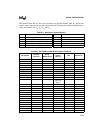
Table B-6. Signal Descriptions (Continued)
Name Type Description