


8XC196MC, MD, MH USER’S MANUAL
5-42
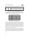
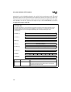
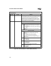
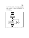
Register Location Function
DATA PTSCB2 + 4 Data Register
This 16-bit register holds the data to be transmitted or the data
that has been received. During transmit mode, the least-
significant bit (bit 0) is transmitted first. Data shifts to the right
with each successive transmission. During receive mode, the
first bit is loaded into the most-significant bit (bit 15). Data shifts
to the right with each successive reception.
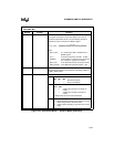
PTSCON1 PTSCB2 + 3 PTS Control Bits
Synchronous Mode
TRC Transmit/Receive Control
0 = transmit or receive data during even numbered
PTS cycles
1 = transmit or receive data during odd numbered PTS
cycles
Initialize this bit at the start of every transmission or
reception.
Asynchronous Mode
RPAR Receive Parity Control and Status
Initialize this bit as indicated before beginning a
reception.
0 = TPAR bit is set to select even parity
1 = TPAR bit is cleared to select odd parity
If this bit is set at the end of a reception, a parity error
has occurred.
PEN Parity Enable
0 = disble parity
1 = enable parity
FE Framing Error Flag
0 = stop bit was 1
1 = stop bit was 0
Clear this bit at the start of every reception.
TPAR Transmit Parity Control
0 = even parity
1 = odd parity
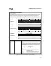
PTS Serial I/O Mode Control Block 2 (Continued)
(8XC196MC, MD)
Figure 5-20. PTS Control Block 2 – Serial I/O Mode (Continued)