2-7
ARCHITECTURAL OVERVIEW
2.4 INTERNAL TIMING
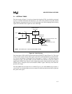
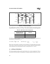
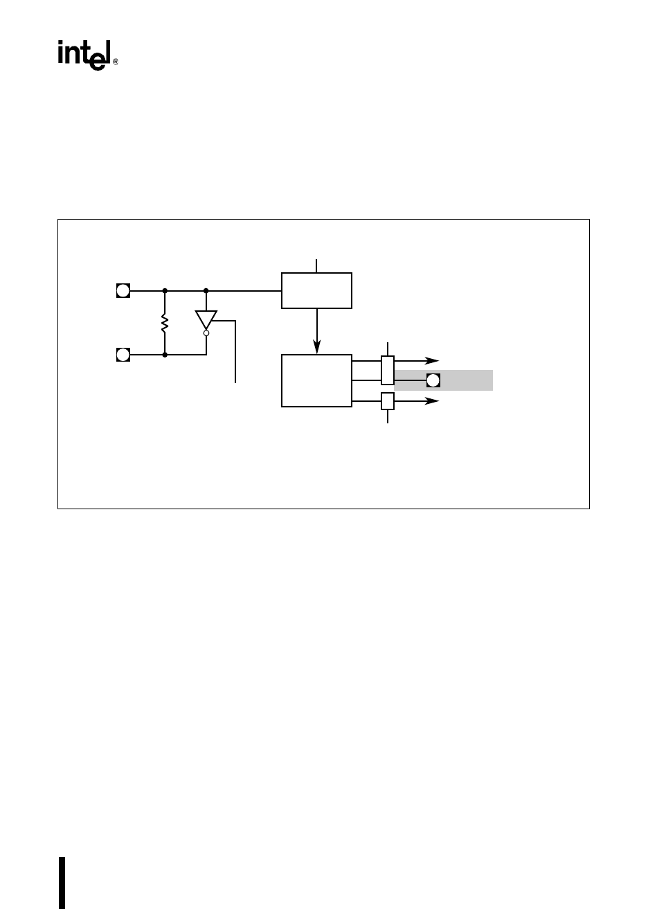
The clock circuitry (Figure 2-3) receives an input clock signal on XTAL1 provided by an external
crystal or oscillator and divides the frequency by two. The clock generators accept the divided
input frequency from the divide-by-two circuit and produce two nonoverlapping internal timing
signals, PH1 and PH2. These signals are active when high.
.
Figure 2-3. Clock Circuitry
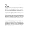
The rising edges of PH1 and PH2 generate the internal CLKOUT signal (Figure 2-4). The clock
circuitry routes separate internal clock signals to the CPU and the peripherals to provide flexibil-
ity in power management. (“Reducing Power Consumption” on page 14-3 describes the power
management modes.) The 8XC196MC and 8XC196MD microcontrollers output the CLKOUT
signal on the CLKOUT pin. Because of the complex logic in the clock circuitry, the signal on the
CLKOUT pin is a delayed version of the internal CLKOUT signal. This delay varies with tem-
perature and voltage.
The 8XC196MH microcontroller has no CLKOUT pin. If your 8XC196MH design requires a
system clock, we recommend that you use an external oscillator and add external logic to generate
the system clock signal.
A3115-02
Clock
Generators
CPU Clocks (PH1, PH2)
Divide-by-two
Circuit
XTAL1
XTAL2
F
XTAL1
Disable
Oscillator
(Powerdown)
Peripheral Clocks (PH1, PH2)
CLKOUT
Disable Clocks
(Powerdown)
Disable Clocks
(Idle, Powerdown)
NOTE: The CLKOUT pin is unique to the 8XC196MC and MD.
Disable Clock Input
(Powerdown)


