


6-17
I/O PORTS
6.5.1 Output-only Port Operation
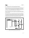
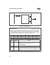
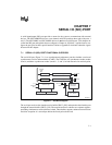
Figure 6-4 shows a simplified circuit schematic for port 6. Port 6 has a single configuration and
control register, WG_OUTPUT. Transistor Q1 can source at least –200 µA at V
CC
–0.3 volts. For
pins P6.0–P6.5, transistor Q2 can sink at least 10 mA at 0.45 volts. For pins P6.6 and P6.7, Q2
can sink at least 200 µA at 0.3 volts.
6.5.2 Configuring Output-only Port Pins
Port 6 has a single configuration register, WG_OUTPUT (Figure 6-5). This register controls the
pin functions, values, and output polarity. This register can be addressed either as a word or as
separate bytes, and it can be windowed. The functions of this register are different for configuring
general-purpose outputs than for configuring waveform generator and PWM outputs.
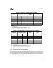
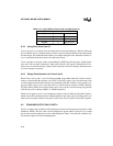
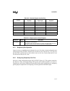
Table 6-14. Standard Output-only Port Pins
Port Pin
Special-function
Signal(s)
Special-function
Signal Type
Associated
Peripheral
P6.0 WG1# Output Waveform generator
P6.1 WG1 Output Waveform generator
P6.2 WG2# Output Waveform generator
P6.3 WG2 Output Waveform generator
P6.4 WG3# Output Waveform generator
P6.5 WG3 Output Waveform generator
P6.6 PWM0 Output PWM
P6.7 PWM1 Output PWM
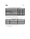
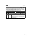
Table 6-15. Output-only Port Control Register
Mnemonic Address Description
WG_OUTPUT 1FC0H Port 6 Output Control Register
This register controls the port 6 pins in I/O mode. Its functions differ when the
port 6 pins are being used as waveform generator or PWM outputs.