


8XC196MC, MD, MH USER’S MANUAL
9-14
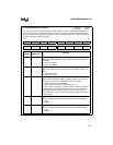
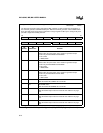
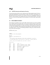
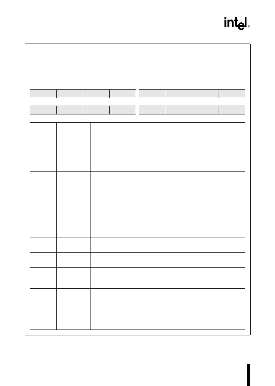
10 PH3.2 Phase 3 Function
Selects either the port function or the waveform generator output
function for pins P6.4/WG3# and P6.5/WG3.
0 = P6.4, P6.5
1 = WG3#, WG3
9 PH2.2 Phase 2 Function
Selects either the port function or the waveform generator output
function for pins P6.2/WG2# and P6.3/WG2.
0 = P6.2, P6.3
1 = WG2#, WG2
8 PH1.2 Phase 1 Function
Selects either the port function or the waveform generator output
function for pins P6.0/WG1# and P6.1/WG1.
0 = P6.0, P6.1
1 = WG1#, WG1
7 P7 P6.7/PWM1 Value
Write the desired P6.7/PWM1 value to this bit.
6 P6 P6.6/PWM0 Value
Write the desired P6.6/PWM0 value to this bit.
5:4 PH3.1:0 P6.4/WG3#, P6.5/WG3 Value
Write the desired output values to these bits. See Table 9-5 on page
9-12.
3:2 PH2.1:0 P6.2/WG2#, P6.3/WG2 Values
Write the desired output values to these bits. See Table 9-5 on page
9-12.
1:0 PH1.1:0 P6.0/WG1#, P6.1/WG1 Values
Write the desired output values to these bits. See Table 9-5 on page
9-12.
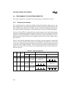
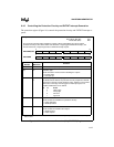
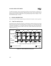
WG_OUTPUT (Waveform Generator) (Continued)
Address:
Reset State:
1FC0H
0000H
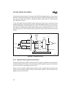
The waveform generator output configuration (WG_OUTPUT) register controls the configuration of
the waveform generator and PWM module pins. Both the waveform generator and the PWM module
share pins with port 6. Having these control bits in a single register enables you to configure all port 6
pins with a single write to WG_OUTPUT.
15 8
OP1 OP0 SYNC PE7 PE6 PH3.2 PH2.2 PH1.2
7 0
P7 P6 PH3.1 PH3.0 PH2.1 PH2.0 PH1.1 PH1.0
Bit
Number
Bit
Mnemonic
Function
Figure 9-8. WG Output Configuration (WG_OUTPUT) Register (Continued)