8XC196MC, MD, MH USER’S MANUAL
15-16
15.3.3 8-bit Bus Timings
When the microcontroller is configured to operate in the 8-bit bus mode, lines AD7:0 form a mul-
tiplexed lower address and data bus. Lines AD15:8 are not multiplexed; the upper address is
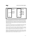
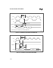
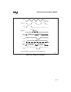
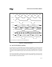
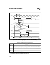
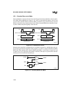
latched and remains valid throughout the bus cycle. Figure 15-7 shows an idealized timing dia-
gram for the external read and write cycles. One cycle is required for an 8-bit read or write. A 16-
bit access requires two cycles. The first cycle accesses the lower byte, and the second cycle ac-
cesses the upper byte. Except for requiring an extra cycle to write the bytes separately, the timings
are the same as on the 16-bit bus.
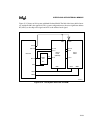
The ALE signal is used to demultiplex the lower address by strobing a transparent latch (such as
a 74AC373).
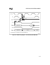
For 8-bit bus read cycles, after ALE falls, the bus controller floats the bus and drives the RD#
signal low. The external memory then must put its data on the bus. That data must be valid at the
rising edge of the RD# signal. To read a data word, the bus controller performs two consecutive
reads, reading the low byte first, followed by the high byte.
For 8-bit bus write cycles, after ALE falls, the bus controller outputs data on AD7:0 and then
drives WR# low. The external memory must latch the data by the time WR# goes high. That data
will be valid on the bus until slightly after WR# goes high. To write a data word, the bus controller
performs two consecutive writes, writing the low byte first, followed by the high byte.


