© Koninklijke Philips Electronics N.V. 2005. All rights reserved.
User manual Rev. 02 — 23 May 2005 94 of 133
Philips Semiconductors
UM10109
P89LPC932A1 User manual
When each comparator is first enabled, the comparator output and interrupt flag are not
guaranteed to be stable for 10 microseconds. The corresponding comparator interrupt
should not be enabled during that time, and the comparator interrupt flag must be cleared
before the interrupt is enabled in order to prevent an immediate interrupt service.
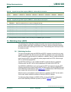
Table 78: Comparator Control register (CMP1 - address ACh, CMP2 - address ADh) bit
allocation
Bit 7 6 5 4 3 2 1 0
Symbol - - CEn CPn CNn OEn COn CMFn
Resetxx000000
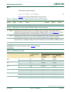
Table 79: Comparator Control register (CMP1 - address ACh, CMP2 - address ADh) bit
description
Bit Symbol Description
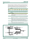
0 CMFn Comparator interrupt flag. This bit is set by hardware whenever the comparator
output COn changes state. This bit will cause a hardware interrupt if enabled.
Cleared by software.
1 COn Comparator output, synchronized to the CPU clock to allow reading by software.
2 OEn Output enable. When logic 1, the comparator output is connected to the CMPn pin
if the comparator is enabled (CEn = 1). This output is asynchronous to the CPU
clock.
3 CNn Comparator negative input select. When logic 0, the comparator reference pin
CMPREF is selected as the negative comparator input. When logic 1, the internal
comparator reference, Vref, is selected as the negative comparator input.
4 CPn Comparator positive input select. When logic 0, CINnA is selected as the positive
comparator input. When logic 1, CINnB is selected as the positive comparator
input.
5 CEn Comparator enable. When set, the corresponding comparator function is enabled.
Comparator output is stable 10 microseconds after CEn is set.
6:7 - reserved
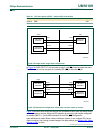
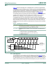
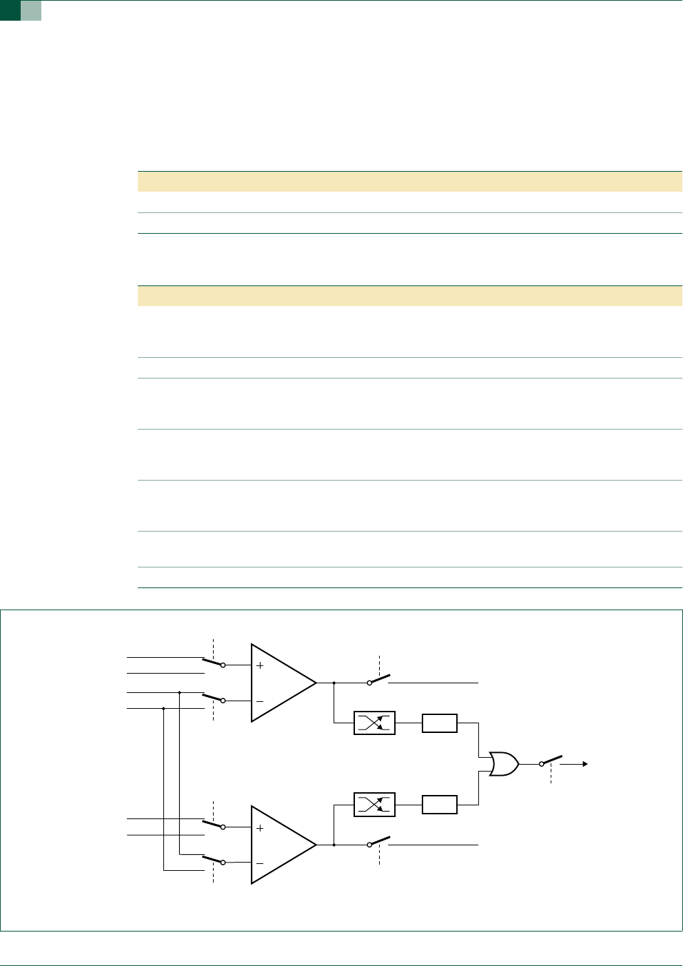
Fig 45. Comparator input and output connections.
comparator 1
CP1
CN1
(P0.4) CIN1A
(P0.3) CIN1B
(P0.5) CMPREF
V
REF
OE1
change detect
CO1
CMF1
interrupt
002aaa904
CMP1 (P0.6)
EC
change detect
CMF2
comparator 2
OE2
CO2
CMP2 (P0.0)
CP2
CN2
(P0.2) CIN2A
(P0.1) CIN2B


