


© Koninklijke Philips Electronics N.V. 2005. All rights reserved.
User manual Rev. 02 — 23 May 2005 89 of 133
Philips Semiconductors
UM10109
P89LPC932A1 User manual
slave and start sending data to it. To avoid bus contention, the SPI becomes a slave. As a
result of the SPI becoming a slave, the MOSI and SPICLK pins are forced to be an input
and MISO becomes an output.
The SPIF flag in SPSTAT is set, and if the SPI interrupt is enabled, an SPI interrupt will
occur.
User software should always check the MSTR bit. If this bit is cleared by a slave select
and the user wants to continue to use the SPI as a master, the user must set the MSTR bit
again, otherwise it will stay in slave mode.
12.5 Write collision
The SPI is single buffered in the transmit direction and double buffered in the receive
direction. New data for transmission can not be written to the shift register until the
previous transaction is complete. The WCOL (SPSTAT.6) bit is set to indicate data
collision when the data register is written during transmission. In this case, the data
currently being transmitted will continue to be transmitted, but the new data, i.e., the one
causing the collision, will be lost.
While write collision is detected for both a master or a slave, it is uncommon for a master
because the master has full control of the transfer in progress. The slave, however, has no
control over when the master will initiate a transfer and therefore collision can occur.
For receiving data, received data is transferred into a parallel read data buffer so that the
shift register is free to accept a second character. However, the received character must
be read from the Data Register before the next character has been completely shifted in.
Otherwise. the previous data is lost.
WCOL can be cleared in software by writing a logic 1 to the bit.
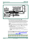
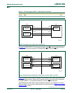
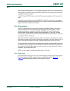
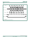
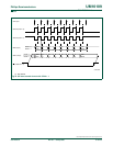
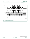
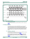
12.6 Data mode
Clock Phase Bit (CPHA) allows the user to set the edges for sampling and changing data.
The Clock Polarity bit, CPOL, allows the user to set the clock polarity. Figure 41
-
Figure 44
show the different settings of Clock Phase bit CPHA.