


© Koninklijke Philips Electronics N.V. 2005. All rights reserved.
User manual Rev. 02 — 23 May 2005 84 of 133
Philips Semiconductors
UM10109
P89LPC932A1 User manual
The SPI interface has four pins: SPICLK, MOSI, MISO and SS:
• SPICLK, MOSI and MISO are typically tied together between two or more SPI
devices. Data flows from master to slave on the MOSI (Master Out Slave In) pin and
flows from slave to master on the MISO (Master In Slave Out) pin. The SPICLK signal
is output in the master mode and is input in the slave mode. If the SPI system is
disabled, i.e. SPEN (SPCTL.6) = 0 (reset value), these pins are configured for port
functions.
• SS is the optional slave select pin. In a typical configuration, an SPI master asserts
one of its port pins to select one SPI device as the current slave. An SPI slave device
uses its SS
pin to determine whether it is selected. The SS is ignored if any of the
following conditions are true:
– If the SPI system is disabled, i.e. SPEN (SPCTL.6) = 0 (reset value)
– If the SPI is configured as a master, i.e., MSTR (SPCTL.4) = 1, and P2.4 is
configured as an output (via the P2M1.4 and P2M2.4 SFR bits);
– If the SS
pin is ignored, i.e. SSIG (SPCTL.7) bit = 1, this pin is configured for port
functions.
Note that even if the SPI is configured as a master (MSTR = 1), it can still be converted to
a slave by driving the SS
pin low (if P2.4 is configured as input and SSIG = 0). Should this
happen, the SPIF bit (SPSTAT.7) will be set (see Section 12.4 “
Mode change on SS”)
Typical connections are shown in Figure 38
to Figure 40.
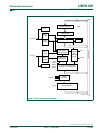
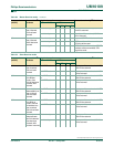
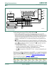
Fig 37. SPI block diagram.
002aaa900
CPU clock
DIVIDER
BY 4, 16, 64, 128
SELECT
CLOCK LOGIC
SPI CONTROL REGISTER
READ DATA BUFFER
8-BIT SHIFT REGISTER
SPI CONTROL
SPI STATUS REGISTER
SPR1
SPIF
WCOL
SPR0
SPI clock (master)
PIN
CONTROL
LOGIC
S
M
S
M
M
S
MISO
P2.3
MOSI
P2.2
SPICLK
P2.5
SS
P2.4
SPI
interrupt
request
internal
data
bus
SSIG
SPEN
SPEN
MSTR
DORD
MSTR
CPHA
CPOL
SPR1
SPR0
MSTR
SPEN
clock
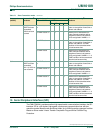
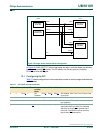
Table 72: SPI Control register (SPCTL - address E2h) bit allocation
Bit 7 6 5 4 3 2 1 0
Symbol SSIG SPEN DORD MSTR CPOL CPHA SPR1 SPR0
Reset00000100