© Koninklijke Philips Electronics N.V. 2005. All rights reserved.
User manual Rev. 02 — 23 May 2005 29 of 133
Philips Semiconductors
UM10109
P89LPC932A1 User manual
(Please refer to the P89LPC932A1 data sheet, Dynamic characteristics for glitch filter
specifications).
4.3 Open drain output configuration
The open drain output configuration turns off all pull-ups and only drives the pull-down
transistor of the port pin when the port latch contains a logic 0. To be used as a logic
output, a port configured in this manner must have an external pull-up, typically a resistor
tied to V
DD
. The pull-down for this mode is the same as for the quasi-bidirectional mode.
The open drain port configuration is shown in Figure 10
.
An open drain port pin has a Schmitt-triggered input that also has a glitch suppression
circuit.
Please refer to the P89LPC932A1 data sheet, Dynamic characteristics for glitch filter
specifications.
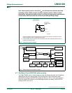
Fig 9. Quasi-bidirectional output.
002aaa914
2 CPU
CLOCK DELAY
port latch
data
weakstrong
input
data
very
weak
PP P
V
DD
PORT
PIN
glitch rejection
Fig 10. Open drain output.
002aaa915
port latch
data
input
data
glitch rejection
PORT
PIN


