© Koninklijke Philips Electronics N.V. 2005. All rights reserved.
User manual Rev. 02 — 23 May 2005 31 of 133
Philips Semiconductors
UM10109
P89LPC932A1 User manual
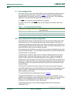
4.6 Port 0 and Analog Comparator functions
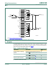
The P89LPC932A1 incorporates two Analog Comparators. In order to give the best
analog performance and minimize power consumption, pins that are being used for
analog functions must have both the digital outputs and digital inputs disabled.
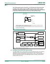
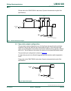
Digital outputs are disabled by putting the port pins into the input-only mode as described
in the Port Configurations section (see Figure 11
).
Digital inputs on Port 0 may be disabled through the use of the PT0AD register. Bits 1
through 5 in this register correspond to pins P0.1 through P0.5 of Port 0, respectively.
Setting the corresponding bit in PT0AD disables that pin’s digital input. Port bits that have
their digital inputs disabled will be read as 0 by any instruction that accesses the port.
On any reset, PT0AD bits 1 through 5 default to logic 0s to enable the digital functions.
4.7 Additional port features
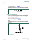
After power-up, all pins are in Input-Only mode. Please note that this is different from
the LPC76x series of devices.
• After power-up, all I/O pins except P1.5, may be configured by software.
• Pin P1.5 is input only. Pins P1.2 and P1.3 are configurable for either input-only or
open drain.
Every output on the P89LPC932A1 has been designed to sink typical LED drive current.
However, there is a maximum total output current for all ports which must not be
exceeded. Please refer to the P89LPC932A1 data sheet for detailed specifications.
All ports pins that can function as an output have slew rate controlled outputs to limit noise
generated by quickly switching output signals. The slew rate is factory-set to
approximately 10 ns rise and fall times.
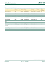
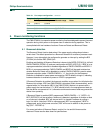
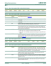
Table 10: Port output configuration
Port pin Configuration SFR bits
PxM1.y PxM2.y Alternate usage Notes
P0.0 P0M1.0 P0M2.0 KBIO, CMP2
P0.1 P0M1.1 P0M2.1 KBI1, CIN2B Refer to Section 4.6 “
Port 0 and
Analog Comparator functions” for
usage as analog inputs.
P0.2 P0M1.2 P0M2.2 KBI2, CIN2A
P0.3 P0M1.3 P0M2.3 KBI3, CIN1B
P0.4 P0M1.4 P0M2.4 KBI4, CIN1A
P0.5 P0M1.5 P0M2.5 KBI5, CMPREF
P0.6 P0M1.6 P0M2.6 KBI6, CMP1
P0.7 P0M1.7 P0M2.7 KBI7, T1
P1.0 P1M1.0 P1M2.0 TxD
P1.1 P1M1.1 P1M2.1 RxD
P1.2 P1M1.2 P1M2.2 T0, SCL Input-only or open-drain
P1.3 P1M1.3 P1M2.3 INTO
, SDA input-only or open-drain
P1.4 P1M1.4 P1M2.4 INT1
P1.5 P1M1.5 P1M2.5 RST


