


© Koninklijke Philips Electronics N.V. 2005. All rights reserved.
User manual Rev. 02 — 23 May 2005 50 of 133
Philips Semiconductors
UM10109
P89LPC932A1 User manual
will have to set the associated I/O pin to the desired output mode to connect the pin.
(Note: The SFR bits for port pins P2.6, P1.6, P1.7, P2.1 must be set to logic 1 in order for
the compare channel outputs to be visible at the port pins.) When the contents of TH2:TL2
match that of OCRxH:OCRxL, the Timer Output Compare Interrupt Flag - TOCFx is set in
TIFR2. This happens in the CCUCLK cycle after the compare takes place. If EA and the
Timer Output Compare Interrupt Enable bit – TOCIE2x (in TICR2 register), as well as
ECCU bit in IEN1 are all set, the program counter will be vectored to the corresponding
interrupt. The user must manually clear the bit by writing a logic 0 to it.
Two bits in OCCRx, the Output Compare x Mode bits OCMx1 and OCMx0 select what
action is taken when a compare match occurs. Enabled compare actions take place even
if the interrupt is disabled.
In order for a Compare Output Action to occur, the compare values must be within the
counting range of the CCU timer.
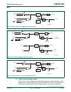
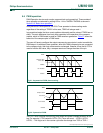
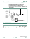
When the compare channel is enabled, the I/O pin (which must be configured as an
output) will be connected to an internal latch controlled by the compare logic. The value of
this latch is zero from reset and can be changed by invoking a forced compare. A forced
compare is generated by writing a logic 1 to the Force Compare x Output bit – FCOx bit in
OCCRx. Writing a one to this bit generates a transition on the corresponding I/O pin as set
up by OCMx1/OCMx0 without causing an interrupt. In basic timer operating mode the
FCOx bits always read zero. (Note: This bit has a different function in PWM mode.) When
an output compare pin is enabled and connected to the compare latch, the state of the
compare pin remains unchanged until a compare event or forced compare occurs.
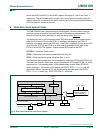
When the user writes to change the output compare value, the values written to OCRH2x
and OCRL2x are transferred to two 8-bit shadow registers. In order to latch the contents of
the shadow registers into the capture compare register, the user must write a logic 1 to the
CCU Timer Compare/Overflow Update bit TCOU2, in the CCU Control Register 1 -
TCR21. The function of this bit depends on whether the timer is running in PWM mode or
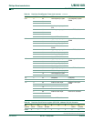
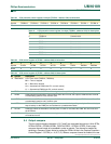
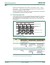
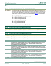
Table 34: Capture compare control register (CCRx - address Exh) bit allocation
Bit 7 6 5 4 3 2 1 0
Symbol ICECx2 ICECx1 ICECx0 ICESx ICNFx FCOx OCMx1 OCMx0
Reset00000000
Table 35: Capture compare control register (CCRx - address Exh) bit description
Bit Symbol Description
0 OCMx0 Output Compare x Mode. See Table 37 “
Output compare pin behavior”
1OCMx1
2 FCOx Force Compare X Output Bit. When set, invoke a force compare.
3 ICNFx Input Capture x Noise Filter Enable Bit. When logic 1, the capture logic needs to see four consecutive
samples of the same value in order to recognize an edge as a capture event. The inputs are sampled
every two CCLK periods regardless of the speed of the timer.
4 ICESx Input Capture x Edge Select Bit. When logic 0: Negative edge triggers a capture, When logic 1: Positive
edge triggers a capture.
5 ICECx0 Capture Delay Setting Bit 0. See Ta ble 36
for details.
6 ICECx1 Capture Delay Setting Bit 1. See Ta ble 36
for details.
7 ICECx2 Capture Delay Setting Bit 2. See Ta ble 36
for details.